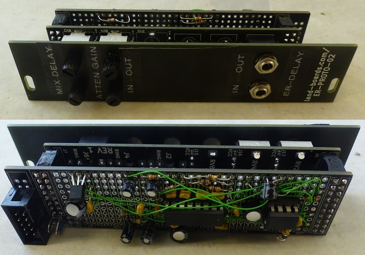
Difference between revisions of "ER-DELAY-01"
Jump to navigation
Jump to search
Blwikiadmin (talk | contribs) (→Videos) |
Blwikiadmin (talk | contribs) |
||
| (55 intermediate revisions by the same user not shown) | |||
| Line 1: | Line 1: | ||
| + | [[File:tindie-mediums.png|link=https://www.tindie.com/products/28896/]] | ||
| + | |||
| + | [[file:ER-DELAY-01_FRONT-BACK-720px.jpg]] | ||
| + | |||
== Features == | == Features == | ||
| Line 9: | Line 13: | ||
* Eurorack 3U, 6HP card | * Eurorack 3U, 6HP card | ||
* Built on [[ER-PROTO-02]] card | * Built on [[ER-PROTO-02]] card | ||
| + | * Input attenuator, output amplifier | ||
* PT2399 has a maximum current of 30mA | * PT2399 has a maximum current of 30mA | ||
* Jacks | * Jacks | ||
| Line 14: | Line 19: | ||
** J6 OUT | ** J6 OUT | ||
* Controls | * Controls | ||
| − | ** RV1 In/Out mix | + | ** RV1 - In/Out mix |
| − | ** RV2 Delay Length | + | ** RV2 - Delay Length |
| + | ** RV3 - Input Attenuator | ||
| + | ** RV4 - Output Gain | ||
* 10 pin Eurorack power jack | * 10 pin Eurorack power jack | ||
| + | ** Uses +12V only | ||
== Design == | == Design == | ||
| Line 29: | Line 37: | ||
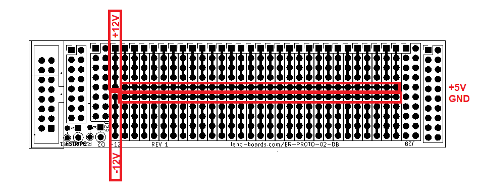
[[FILE:ER-PROTO-02-DB_REAR_PWR.png]] | [[FILE:ER-PROTO-02-DB_REAR_PWR.png]] | ||
| − | === | + | === Card Build === |
| − | + | * Controls card rear | |
| − | === PT2399 Delay IC === | + | [[FILE:ER-DELAY-01_P1090138-720px.jpg]] |
| + | |||
| + | * Partly built | ||
| + | |||
| + | [[FILE:ER-DELAY-01_P1090064-720px.jpg]] | ||
| + | |||
| + | * PT2399 Pin 1 on bottom left | ||
| + | |||
| + | [[FILE:ER-DELAY-01_P1090064-part-720px.jpg]] | ||
| + | |||
| + | * Daughtercard | ||
| + | |||
| + | [[FILE:ER-DELAY-01_P1090134-720px.jpg]] | ||
| + | |||
| + | * Back of daughtercard | ||
| + | |||
| + | [[FILE:ER-DELAY-01_P1090137-720px.jpg]] | ||
| + | |||
| + | * Card Stackup | ||
| + | |||
| + | [[FILE:ER-DELAY-01_P1090135-720px.jpg]] | ||
| + | |||
| + | * Front view | ||
| + | |||
| + | [[FILE:ER-DELAY-01_P1090130-720px.jpg]] | ||
| + | |||
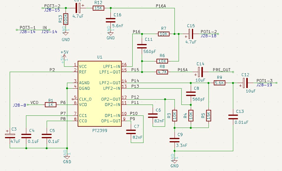
| + | === U1 - PT2399 Delay IC === | ||
[[file:ER-DELAY-01_U1_P2399.PNG]] | [[file:ER-DELAY-01_U1_P2399.PNG]] | ||
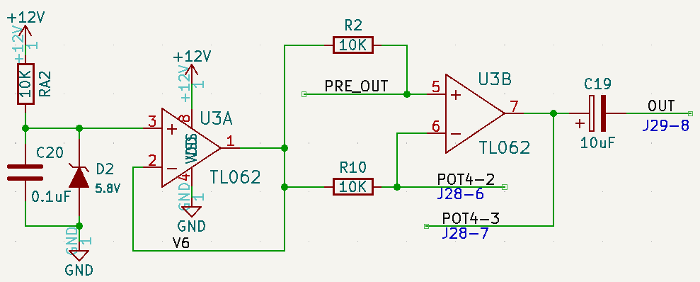
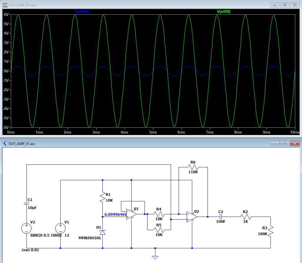
| − | === Pots connector on Daughtercard === | + | === U3 - Output Amplifier === |
| + | |||
| + | * [https://www.analog.com/en/analog-dialogue/articles/avoiding-op-amp-instability-problems.html Avoiding Op-Amp Instability Problems In Single-Supply Applications] | ||
| + | |||
| + | [[file:ER-DELAY-01_OUT-AMP.PNG]] | ||
| + | |||
| + | * [https://github.com/land-boards/lb-boards/tree/master/SYNTHS/ER-PROTO-02_SET/ER-DELAY-01/Docs/OUTPUT LTSpice Simulation] | ||
| + | |||
| + | [[file:OUT_AMP_01.PNG]] | ||
| + | |||
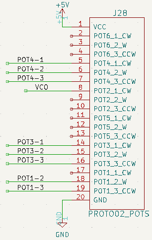
| + | === J28 - Pots connector on Daughtercard === | ||
[[file:ER-DELAY-01_J28_POTS.PNG]] | [[file:ER-DELAY-01_J28_POTS.PNG]] | ||
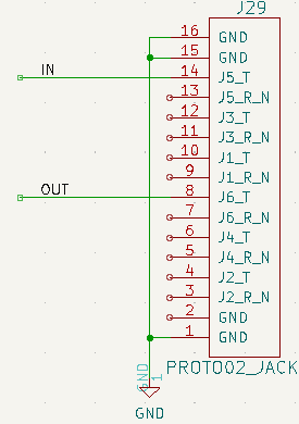
| − | === Jacks connector on Daughtercard === | + | === J29 - Jacks connector on Daughtercard === |
[[file:ER-DELAY-01_J29_JACKS.PNG]] | [[file:ER-DELAY-01_J29_JACKS.PNG]] | ||
| − | === Power connector on Daughtercard === | + | === J9/J15 - Power connector on Daughtercard === |
| − | [[file:ER-DELAY- | + | [[file:ER-DELAY-01_J9_POWER.PNG]] |
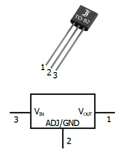
| − | === 5V Power Regulator === | + | ==== U2 - 5V Power Regulator ==== |
[[file:78L05_pkg.PNG]] | [[file:78L05_pkg.PNG]] | ||
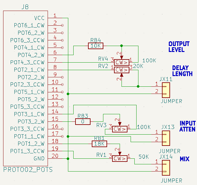
| − | === Pots connector on Controls card === | + | === J8 - Pots connector on Controls card === |
[[file:ER-DELAY-01_J8_CTRL_POTS.PNG]] | [[file:ER-DELAY-01_J8_CTRL_POTS.PNG]] | ||
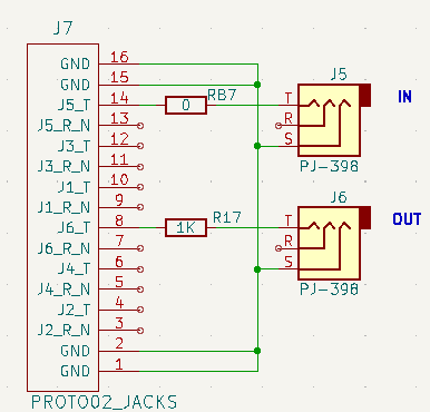
| − | === Pots connector on Controls card === | + | === J7 - Pots connector on Controls card === |
[[file:ER-DELAY-01_J7_CTRL_JACKS.PNG]] | [[file:ER-DELAY-01_J7_CTRL_JACKS.PNG]] | ||
| + | |||
| + | == Schematic == | ||
| + | |||
| + | *[https://github.com/land-boards/lb-boards/blob/master/SYNTHS/ER-PROTO-02_SET/ER-DELAY-01/ER-DELAY-01_Schematic.pdf Schematic] | ||
== Nets == | == Nets == | ||
| Line 109: | Line 157: | ||
Net-(RB1-Pad1),RB1-1,RV1-2, | Net-(RB1-Pad1),RB1-1,RV1-2, | ||
</pre> | </pre> | ||
| + | |||
| + | * [https://www.madbeanpedals.com/forum/index.php?topic=29430.0 Glam Chorus with Vibe Mod] | ||
| + | |||
| + | == Measurements == | ||
| + | |||
| + | * Bass Drum echo | ||
| + | |||
| + | [[file:ER-DELAY-01_MEASURE-001.png]] | ||
| + | |||
| + | * Both Mix/Length knobs full CCW | ||
| + | |||
| + | [[file:ER-DELAY-01_MEASURE-002.png]] | ||
| + | |||
| + | * All (4) drum triggers on IN | ||
| + | |||
| + | [[FILE:ER-DELAY-01_MEASURE-004_ALL-DRUMS.png]] | ||
| + | |||
| + | == Reference == | ||
| + | |||
| + | * [https://www.madbeanpedals.com/forum/index.php?topic=29430.0 Little Angel Chorus] | ||
| + | * [https://www.analog.com/en/analog-dialogue/articles/avoiding-op-amp-instability-problems.html Avoiding Op-Amp Instability Problems In Single-Supply Applications] | ||
| + | * [https://www.synthrotek.com/kit-assembly-instructions/lofi-synth-kits/pt2399-dev-delay-assembly-instructions/ PT2399 Dev Delay Assembly Instructions] | ||
| + | * [https://www.synthrotek.com/kit-assembly-instructions/lofi-synth-kits/pt2399-dev-delay-assembly-instructions/pt2399-dev-board-bom/ PT2399 Dev Delay BOM] | ||
| + | * [https://store.synthrotek.com/PT2399_Dev_Delay_PCB_ONLY PT2399 Dev Delay PCB] | ||
| + | * [https://note.com/solder_state/n/nf6dc0a61e26d HAGIWO PT2399 clock sync delay] | ||
| + | * [https://www.electrosmash.com/pt2399-analysis PT2399 Analysis bu Electrosmash] | ||
| + | * [https://electricdruid.net/useful-design-equations-for-the-pt2399/ Useful design equations for the PT2399] | ||
| + | * [http://musicfromouterspace.com/analogsynth_new/ECHOFXXX/ECHOFXXX.php MFOS ECHOFXXX] | ||
| + | * [http://www.valvewizard.co.uk/PT2399_Data_Notes.pdf Valve Wizard Additional notes] | ||
| + | * [https://www.schmitzbits.de/pt2399.html schmitzbits PT2399 based Delay] | ||
| + | * [https://benjiaomodular.com/post/2022-09-11-mini-delay/ benjiaomodular MiniDelay] | ||
== Videos == | == Videos == | ||
| Line 115: | Line 194: | ||
<video type="youtube">W8bB5ZQk2As</video> | <video type="youtube">W8bB5ZQk2As</video> | ||
| + | |||
| + | <video type="youtube">DvKIe1b04PU</video> | ||
Latest revision as of 17:53, 18 February 2023
Contents
- 1 Features
- 2 Design
- 2.1 Daughtercard Prototyping Area
- 2.2 Card Build
- 2.3 U1 - PT2399 Delay IC
- 2.4 U3 - Output Amplifier
- 2.5 J28 - Pots connector on Daughtercard
- 2.6 J29 - Jacks connector on Daughtercard
- 2.7 J9/J15 - Power connector on Daughtercard
- 2.8 J8 - Pots connector on Controls card
- 2.9 J7 - Pots connector on Controls card
- 3 Schematic
- 4 Nets
- 5 Measurements
- 6 Reference
- 7 Videos
Features
- PT2399 Delay/Echo
- The PT2399 is a CMOS single-chip echo processor IC
- A high sample rate ADC converts the analog data into a bitstream, which is then stored in internal 44Kbit RAM
- After processing, the bitstream is de-modulated by DAC and lowpass filter
- The internal VCO clock frequency determines the overall delay duration
- The user can easily modify the VCO frequency by changing the external resistance
- Eurorack 3U, 6HP card
- Built on ER-PROTO-02 card
- Input attenuator, output amplifier
- PT2399 has a maximum current of 30mA
- Jacks
- J5 IN
- J6 OUT
- Controls
- RV1 - In/Out mix
- RV2 - Delay Length
- RV3 - Input Attenuator
- RV4 - Output Gain
- 10 pin Eurorack power jack
- Uses +12V only
Design
- ER-PROTO-02 card set
- Front Panel
- Controls Card
- Daughtercard
Daughtercard Prototyping Area
Card Build
- Controls card rear
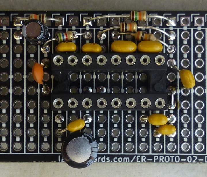
- Partly built
- PT2399 Pin 1 on bottom left
- Daughtercard
- Back of daughtercard
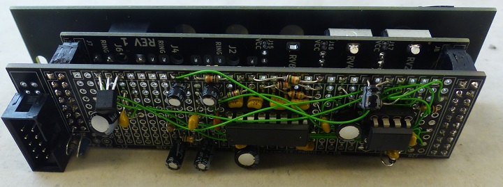
- Card Stackup
- Front view
U1 - PT2399 Delay IC
U3 - Output Amplifier
J28 - Pots connector on Daughtercard
J29 - Jacks connector on Daughtercard
J9/J15 - Power connector on Daughtercard
U2 - 5V Power Regulator
J8 - Pots connector on Controls card
J7 - Pots connector on Controls card
Schematic
Nets
+5V,C10-1,C18-1,J28-1,U1-1,U2-1,
+12V,C1-1,C2-1,D1-1,J15-1,J15-2,J15-3,J15-4,J15-5,U2-3,
+12VA,J9-10,J9-9,RA1-2,
/IN,C17-2,J29-14,R13-2,
/J4-T,J29-6,
/OUT,C14-2,J29-8,
/P2,C3-1,U1-2,
/P6,R1-1,U1-6,
/P7,C4-1,U1-7,
/P8,C5-1,U1-8,
/P9,C7-1,U1-9,
/P10,C7-2,U1-10,
/P11,C6-1,U1-11,
/P12,C6-2,R3-2,U1-12,
/P13,C8-2,R4-2,U1-13,
/P14,C8-1,R5-2,R9-1,U1-14,
/P15,C11-2,R6-1,R8-1,U1-15,
/P15A,C14-1,R8-2,
/P16,C11-1,R7-1,U1-16,
/P16A,C15-1,C16-1,R12-2,R6-2,R7-2,
/POT1-2,C15-2,J28-18,
/POT1-3,C12-2,J28-19,
/POT3-1,J28-14,
/POT3-2,J28-15,
/POT3-3,J28-16,
/VCO,J28-8,R1-2,
GND,C1-2,C10-2,C13-2,C16-2,C18-2,C2-2,C3-2,C4-2,C5-2,C9-2,J28-20,J29-1,J29-15,J29-16,J9-3,J9-4,J9-5,J9-6,J9-7,J9-8,R13-1,U1-3,U1-4,U2-2,
Net-(C9-Pad1),C9-1,R3-1,R4-1,R5-1,
Net-(C12-Pad1),C12-1,C13-1,R9-2,
Net-(C17-Pad1),C17-1,R12-1,
Net-(D1-Pad2),D1-2,RA1-1,
Net-(J5-PadS),J5-S,J6-R,J7-15,J7-16,
Net-(J5-PadT),J5-T,RB7-1,
Net-(J6-PadS),J6-S,J7-1,J7-2,
Net-(J6-PadT),J6-T,R17-1,
Net-(J7-Pad8),J7-8,R17-2,
Net-(J7-Pad14),J7-14,RB7-2,
Net-(J8-Pad8),J8-8,RV2-1,
Net-(J8-Pad18),J8-18,RB1-2,
Net-(J8-Pad19),J8-19,RV1-3,
Net-(J11-Pad1),J11-1,RV2-2,RV2-3,
Net-(J11-Pad2),J11-2,J14-2,J8-1,J8-20,
Net-(J14-Pad1),J14-1,RV1-1,
Net-(RB1-Pad1),RB1-1,RV1-2,
Measurements
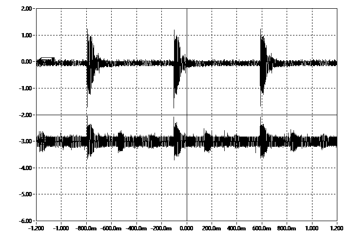
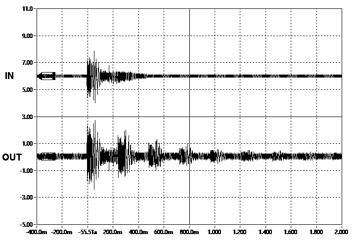
- Bass Drum echo
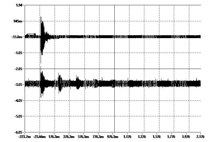
- Both Mix/Length knobs full CCW
- All (4) drum triggers on IN
Reference
- Little Angel Chorus
- Avoiding Op-Amp Instability Problems In Single-Supply Applications
- PT2399 Dev Delay Assembly Instructions
- PT2399 Dev Delay BOM
- PT2399 Dev Delay PCB
- HAGIWO PT2399 clock sync delay
- PT2399 Analysis bu Electrosmash
- Useful design equations for the PT2399
- MFOS ECHOFXXX
- Valve Wizard Additional notes
- schmitzbits PT2399 based Delay
- benjiaomodular MiniDelay
Videos
- Kristian Blåsol

