Difference between revisions of "6 Channel Relay Driver Card"
Jump to navigation
Jump to search
Blwikiadmin (talk | contribs) |
Blwikiadmin (talk | contribs) |
||
| (62 intermediate revisions by the same user not shown) | |||
| Line 1: | Line 1: | ||
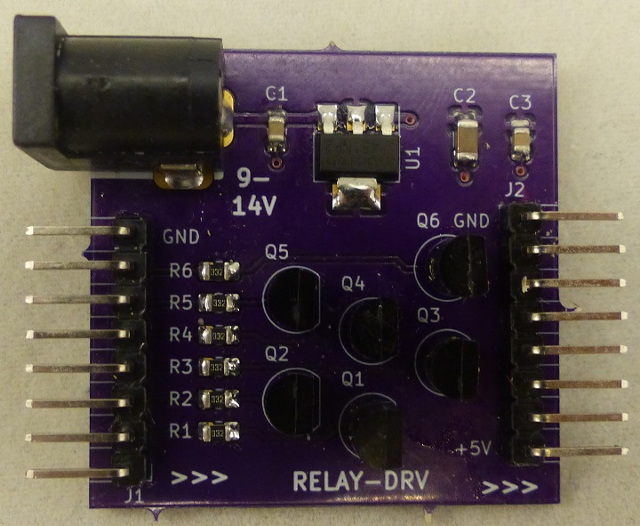
| − | [[FILE: | + | [[FILE:RELAY_DRVE_P1981-720PX.jpg]] |
== Features == | == Features == | ||
| + | * Drives relays on [https://qrp-labs.com/ultimatelpf.html QRP Labs Ultimate relay-switched BPF/LPF kit] | ||
| + | ** Drives either receiver Band Pass (BP) Filters or transmitter Low Pass (LP) Filters | ||
| + | ** Open collector to turn on/off relay | ||
| + | ** Drives low to turn on relay | ||
| + | *** Other side of relay pulled up to 5V | ||
| + | ** User should only turn on one output at a time | ||
* Inputs | * Inputs | ||
| − | ** 6 channels | + | ** 6 channels (5 used with Ultimate Relay Card) |
** Active-high in to drive relay to on state | ** Active-high in to drive relay to on state | ||
| − | ** | + | ** 3.3K to transistor base |
| − | *** | + | *** 1 mA for 3.3V drive |
| − | *** | + | *** 1.5 mA for 5V drive |
| + | * Outputs | ||
| + | ** Open Collector outputs from [https://media.digikey.com/pdf/Data%20Sheets/NXP%20PDFs/2N3904.pdf 2N3904] NPN transistors | ||
* Power | * Power | ||
| − | ** 9- | + | ** 9-14V power in |
** 5V power out to power relays | ** 5V power out to power relays | ||
** DC jack | ** DC jack | ||
* 36x37mm card | * 36x37mm card | ||
** 3 PCBs for $11 from OshPark | ** 3 PCBs for $11 from OshPark | ||
| + | |||
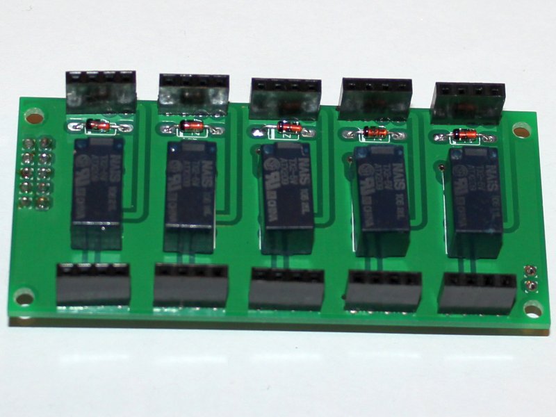
| + | == Ultimate Relay Card == | ||
| + | |||
| + | * [https://qrp-labs.com/ultimatelpf.html Ultimate relay-switched LPF kit] | ||
| + | ** [https://qrp-labs.com/images/ultimatelpf/assembly_ulpf2.pdf Ultimate relay-switched LPF kit Build Instructions] | ||
| + | * Takes five [https://qrp-labs.com/bpfkit.html QRP Labs Bandpass Filters] or [https://qrp-labs.com/lpfkit.html Low Pass Filters] | ||
| + | |||
| + | [[file:Ultimate_Relay_Card_5.jpg]] | ||
| + | |||
| + | === Ultimate Relay Card Connections === | ||
| + | |||
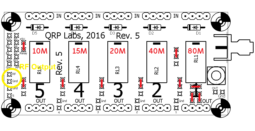
| + | * The RF input is the RFI pin of the 2 x 5-pin header on the left of the board (same as in the Low Pass Filter kit usage) | ||
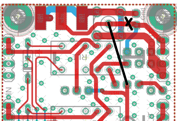
| + | * RF output cut the track from the SMA connector center pins and add a wire to connect it to the common bus track that runs horizontally across the board, finishing at the "RF" pad circled in yellow | ||
| + | * Cut/Jumper | ||
| + | ** Cut on top side near Vertical SMA | ||
| + | ** Jumper on rear side | ||
| + | |||
| + | [[file:SWITCHED_FILTER_Cuts.PNG]] | ||
| + | |||
| + | * Jumpers | ||
| + | |||
| + | === Ultimate Relay Card Jumpers - Band Pass (BP) === | ||
| + | |||
| + | * To switch Band Pass (BP) filters, use the jumper configuration shown below | ||
| + | |||
| + | [[file:jumpers-BPF.gif]] | ||
| + | |||
| + | === Ultimate Relay Card Connectors === | ||
| + | |||
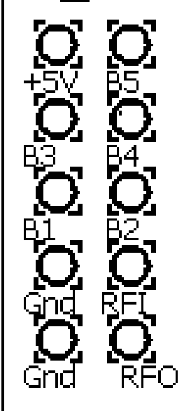
| + | [[file:SWITCHED_FILTER_Conns.PNG]] | ||
| + | |||
| + | # +5V | ||
| + | # B5 | ||
| + | # B3 | ||
| + | # B4 | ||
| + | # B1 | ||
| + | # B2 | ||
| + | # GND | ||
| + | # RFIn | ||
| + | # GND | ||
| + | # RFOut | ||
| + | |||
| + | == Connectors == | ||
| + | |||
| + | === J1 - Input Connector === | ||
| + | |||
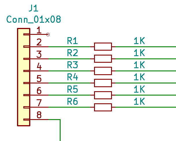
| + | [[FILE:RELAY_DRVR_J1.PNG]] | ||
| + | |||
| + | # N/C | ||
| + | # IN1 | ||
| + | # IN2 | ||
| + | # IN3 | ||
| + | # IN4 | ||
| + | # IN5 | ||
| + | # IN6 | ||
| + | # GND | ||
| + | |||
| + | === J2 - Output Connector === | ||
| + | |||
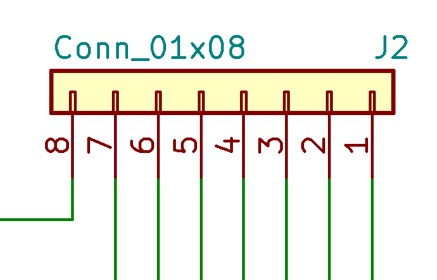
| + | [[FILE:RELAY_DRVR_J2.PNG]] | ||
| + | |||
| + | # GND | ||
| + | # OUT6 | ||
| + | # OUT5 | ||
| + | # OUT4 | ||
| + | # OUT3 | ||
| + | # OUT2 | ||
| + | # OUT1 | ||
| + | # 5V OUT | ||
| + | |||
| + | === Power Connector === | ||
| + | |||
| + | * 7-14V input | ||
| + | * Center positive | ||
| + | |||
| + | == Control via VFO-003 == | ||
| + | |||
| + | * [[VFO-003]] | ||
| + | ** Band select via menu option | ||
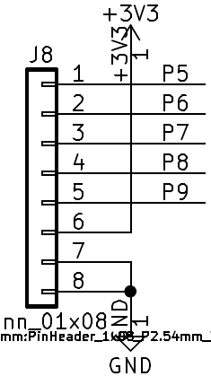
| + | * J8 - Arduino P5-P9 | ||
| + | * Arduino pins | ||
| + | |||
| + | # Arduino D5 - 10M select | ||
| + | # Arduino D6 - 15M select | ||
| + | # Arduino D7 - 20M select | ||
| + | # Arduino D8 - 40M select | ||
| + | # Arduino D9 - 80M select | ||
| + | # Vcc | ||
| + | # GND | ||
| + | # GND | ||
| + | |||
| + | [[file:VFO-003_J8.PNG]] | ||
| + | |||
| + | == Cables == | ||
| + | |||
| + | === VFO-003 to Relay Driver Card === | ||
| + | |||
| + | {| class="wikitable" | ||
| + | ! RLY_DRVR pin | ||
| + | 1x8 BERG | ||
| + | ! Signal | ||
| + | ! Function | ||
| + | ! VFO-003_Pin | ||
| + | 1x8 BERG | ||
| + | |- | ||
| + | | 1 | ||
| + | | N/C | ||
| + | | N/C | ||
| + | | | ||
| + | |- | ||
| + | | 2 | ||
| + | | IN1 | ||
| + | | 10M | ||
| + | | 1 | ||
| + | |- | ||
| + | | 3 | ||
| + | | IN2 | ||
| + | | 15M | ||
| + | | 2 | ||
| + | |- | ||
| + | | 4 | ||
| + | | IN3 | ||
| + | | 20M | ||
| + | | 3 | ||
| + | |- | ||
| + | | 5 | ||
| + | | IN4 | ||
| + | | 40M | ||
| + | | 4 | ||
| + | |- | ||
| + | | 6 | ||
| + | | IN5 | ||
| + | | 80M | ||
| + | | 5 | ||
| + | |- | ||
| + | | 7 | ||
| + | | IN6 | ||
| + | | N/C | ||
| + | | | ||
| + | |- | ||
| + | | 8 | ||
| + | | GND | ||
| + | | GND | ||
| + | | 7 | ||
| + | |- | ||
| + | |} | ||
| + | |||
| + | === Relay Driver to Relay Card === | ||
| + | |||
| + | {| class="wikitable" | ||
| + | ! RLY pin | ||
| + | 2x5 BERG | ||
| + | ! Signal | ||
| + | ! Function | ||
| + | ! RLY_DRVR pin | ||
| + | 1x8 BERG | ||
| + | ! Signal | ||
| + | |- | ||
| + | | 1 | ||
| + | | +5V | ||
| + | | Power | ||
| + | | 8 | ||
| + | | 5V | ||
| + | |- | ||
| + | | 2 | ||
| + | | B5 | ||
| + | | 80M | ||
| + | | 3 | ||
| + | | OUT5 | ||
| + | |- | ||
| + | | 3 | ||
| + | | B3 | ||
| + | | 20M | ||
| + | | 5 | ||
| + | | OUT3 | ||
| + | |- | ||
| + | | 4 | ||
| + | | B4 | ||
| + | | 40M | ||
| + | | 4 | ||
| + | | OUT4 | ||
| + | |- | ||
| + | | 5 | ||
| + | | B1 | ||
| + | | 10M | ||
| + | | 7 | ||
| + | | OUT1 | ||
| + | |- | ||
| + | | 6 | ||
| + | | B2 | ||
| + | | 15M | ||
| + | | 6 | ||
| + | | OUT2 | ||
| + | |- | ||
| + | | 7 | ||
| + | | GND | ||
| + | | RF Gnd | ||
| + | | N/C | ||
| + | | GND | ||
| + | |- | ||
| + | | 8 | ||
| + | | RFI | ||
| + | | RF In | ||
| + | | N/C | ||
| + | | | ||
| + | |- | ||
| + | | 9 | ||
| + | | GND | ||
| + | | Power | ||
| + | | 1 | ||
| + | | GND | ||
| + | |- | ||
| + | | 10 | ||
| + | | RFO | ||
| + | | N/C | ||
| + | | N/C | ||
| + | | | ||
| + | |- | ||
| + | | | ||
| + | | | ||
| + | | | ||
| + | | 2 | ||
| + | | N/C | ||
| + | |- | ||
| + | |} | ||
| + | |||
| + | == Testing == | ||
| + | |||
| + | * Apply 9-12V to DC jack | ||
| + | * Use LED w/ resistor on output to check 5V | ||
| + | * One channel at a time | ||
| + | ** Pull up channel input to +5V | ||
| + | ** Check output with LED pulled up to +5V out | ||
== CAD == | == CAD == | ||
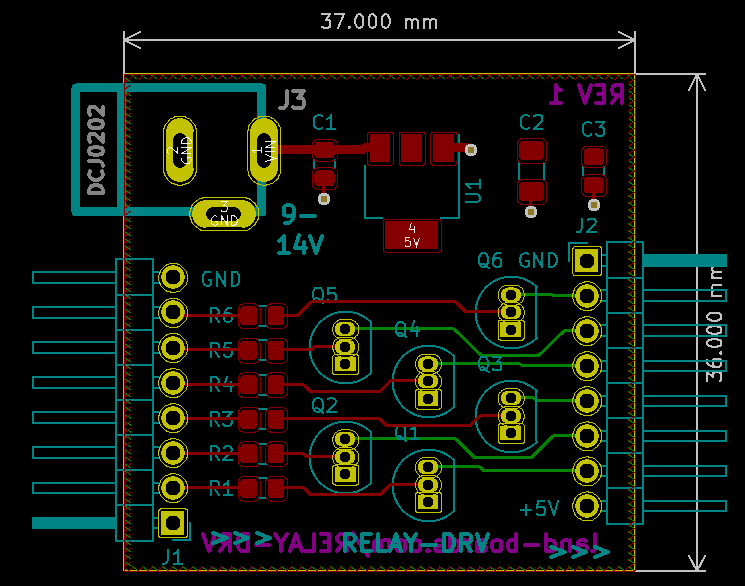
[[FILE:RELAY-DRV_CAD.PNG]] | [[FILE:RELAY-DRV_CAD.PNG]] | ||
Latest revision as of 18:53, 27 January 2022
Contents
Features
- Drives relays on QRP Labs Ultimate relay-switched BPF/LPF kit
- Drives either receiver Band Pass (BP) Filters or transmitter Low Pass (LP) Filters
- Open collector to turn on/off relay
- Drives low to turn on relay
- Other side of relay pulled up to 5V
- User should only turn on one output at a time
- Inputs
- 6 channels (5 used with Ultimate Relay Card)
- Active-high in to drive relay to on state
- 3.3K to transistor base
- 1 mA for 3.3V drive
- 1.5 mA for 5V drive
- Outputs
- Open Collector outputs from 2N3904 NPN transistors
- Power
- 9-14V power in
- 5V power out to power relays
- DC jack
- 36x37mm card
- 3 PCBs for $11 from OshPark
Ultimate Relay Card
Ultimate Relay Card Connections
- The RF input is the RFI pin of the 2 x 5-pin header on the left of the board (same as in the Low Pass Filter kit usage)
- RF output cut the track from the SMA connector center pins and add a wire to connect it to the common bus track that runs horizontally across the board, finishing at the "RF" pad circled in yellow
- Cut/Jumper
- Cut on top side near Vertical SMA
- Jumper on rear side
- Jumpers
Ultimate Relay Card Jumpers - Band Pass (BP)
- To switch Band Pass (BP) filters, use the jumper configuration shown below
Ultimate Relay Card Connectors
- +5V
- B5
- B3
- B4
- B1
- B2
- GND
- RFIn
- GND
- RFOut
Connectors
J1 - Input Connector
- N/C
- IN1
- IN2
- IN3
- IN4
- IN5
- IN6
- GND
J2 - Output Connector
- GND
- OUT6
- OUT5
- OUT4
- OUT3
- OUT2
- OUT1
- 5V OUT
Power Connector
- 7-14V input
- Center positive
Control via VFO-003
- VFO-003
- Band select via menu option
- J8 - Arduino P5-P9
- Arduino pins
- Arduino D5 - 10M select
- Arduino D6 - 15M select
- Arduino D7 - 20M select
- Arduino D8 - 40M select
- Arduino D9 - 80M select
- Vcc
- GND
- GND
Cables
VFO-003 to Relay Driver Card
| RLY_DRVR pin
1x8 BERG |
Signal | Function | VFO-003_Pin
1x8 BERG |
|---|---|---|---|
| 1 | N/C | N/C | |
| 2 | IN1 | 10M | 1 |
| 3 | IN2 | 15M | 2 |
| 4 | IN3 | 20M | 3 |
| 5 | IN4 | 40M | 4 |
| 6 | IN5 | 80M | 5 |
| 7 | IN6 | N/C | |
| 8 | GND | GND | 7 |
Relay Driver to Relay Card
| RLY pin
2x5 BERG |
Signal | Function | RLY_DRVR pin
1x8 BERG |
Signal |
|---|---|---|---|---|
| 1 | +5V | Power | 8 | 5V |
| 2 | B5 | 80M | 3 | OUT5 |
| 3 | B3 | 20M | 5 | OUT3 |
| 4 | B4 | 40M | 4 | OUT4 |
| 5 | B1 | 10M | 7 | OUT1 |
| 6 | B2 | 15M | 6 | OUT2 |
| 7 | GND | RF Gnd | N/C | GND |
| 8 | RFI | RF In | N/C | |
| 9 | GND | Power | 1 | GND |
| 10 | RFO | N/C | N/C | |
| 2 | N/C |
Testing
- Apply 9-12V to DC jack
- Use LED w/ resistor on output to check 5V
- One channel at a time
- Pull up channel input to +5V
- Check output with LED pulled up to +5V out
