Difference between revisions of "IOP16 I2C"
Jump to navigation
Jump to search
Blwikiadmin (talk | contribs) (Created page with "== I2C Interface == * The I2C core provides register addresses that the CPU can read or written to ** Address 0 -> DATA (write/read) or SLAVE ADDRESS (write) ** Address 1 -...") |
Blwikiadmin (talk | contribs) (→Timing) |
||
| (2 intermediate revisions by the same user not shown) | |||
| Line 25: | Line 25: | ||
* bit 1 = ERROR (I2C transaction error) | * bit 1 = ERROR (I2C transaction error) | ||
* bit 0 = BUSY (I2C bus busy) | * bit 0 = BUSY (I2C bus busy) | ||
| + | |||
| + | == Timing == | ||
| + | |||
| + | * 400 KHz bit timing | ||
| + | |||
| + | [[file:FRONT_PANEL_READ_WRITE_WORKING_400 KHz-timing.PNG]] | ||
== Example (R32V2020) == | == Example (R32V2020) == | ||
Latest revision as of 19:04, 10 April 2022
Contents
I2C Interface
- The I2C core provides register addresses that the CPU can read or written to
- Address 0 -> DATA (write/read) or SLAVE ADDRESS (write)
- Address 1 -> Command/Status Register (write/read)
Data Buffer (write/read)
- bit 7-0 = Stores I2C read/write data, or
- bit 7-1 = Holds the first seven address bits of the I2C slave device
- bit 0 = I2C 1:read/0:write bit
Command Register (write)
- bit 7-2 = Reserved
- bit 1-0
- 00: IDLE
- 01: START
- 10: nSTART
- 11: STOP
Status Register (read)
- bit 7-2 = Reserved
- bit 1 = ERROR (I2C transaction error)
- bit 0 = BUSY (I2C bus busy)
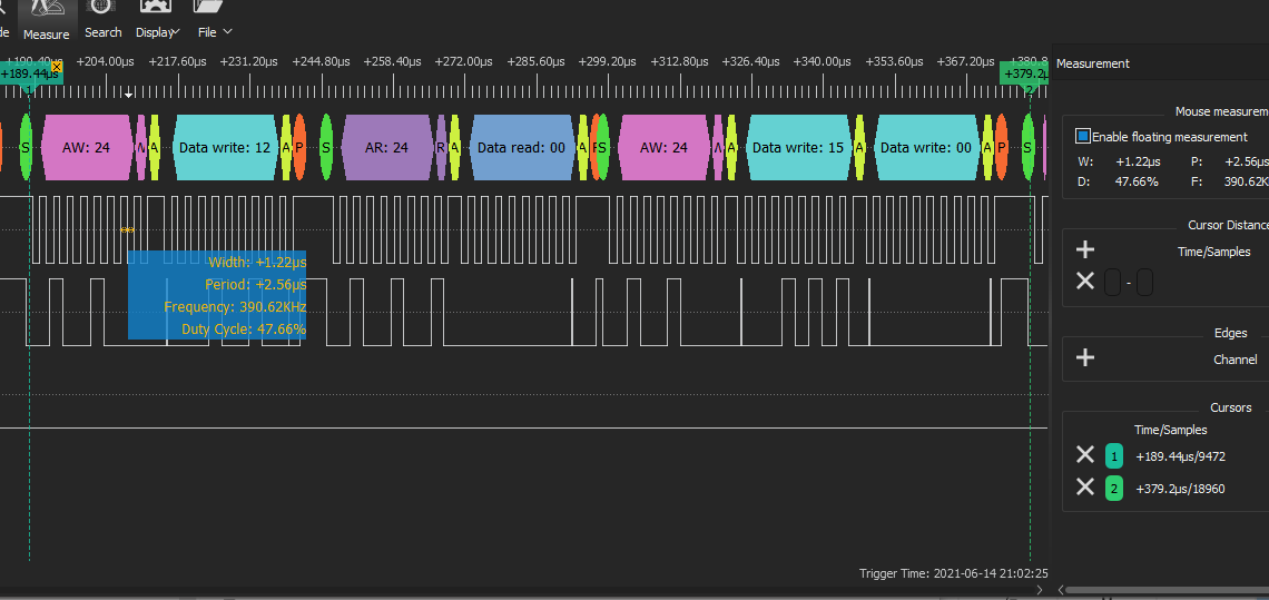
Timing
- 400 KHz bit timing
Example (R32V2020)
; Write 0x22 to IOCON register (not sequential operations)
START
 lix		r8,0x01
 bsr		write_I2C_Ctrl_Reg
; I2C Slave address
 lix		r8,0x40
 bsr		write_I2C_Data_Address_Reg
IDLE
 lix		r8,0x00
 bsr		write_I2C_Ctrl_Reg
; IO control register
 lix		r8,0x05
 bsr		write_I2C_Data_Address_Reg
; STOP
 lix		r8,0x03
 bsr		write_I2C_Ctrl_Reg
; Disable sequential operation
 lix		r8,0x22
 bsr		write_I2C_Data_Address_Reg
