Difference between revisions of "6 Channel Relay Driver Card"
Jump to navigation
Jump to search
Blwikiadmin (talk | contribs) |
Blwikiadmin (talk | contribs) |
||
| Line 23: | Line 23: | ||
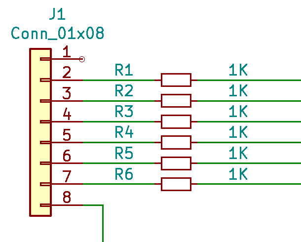
[[FILE:RELAY_DRVR_J1.PNG]] | [[FILE:RELAY_DRVR_J1.PNG]] | ||
| + | |||
| + | # N/C | ||
| + | # IN1 | ||
| + | # IN2 | ||
| + | # IN3 | ||
| + | # IN4 | ||
| + | # IN5 | ||
| + | # IN6 | ||
| + | # GND | ||
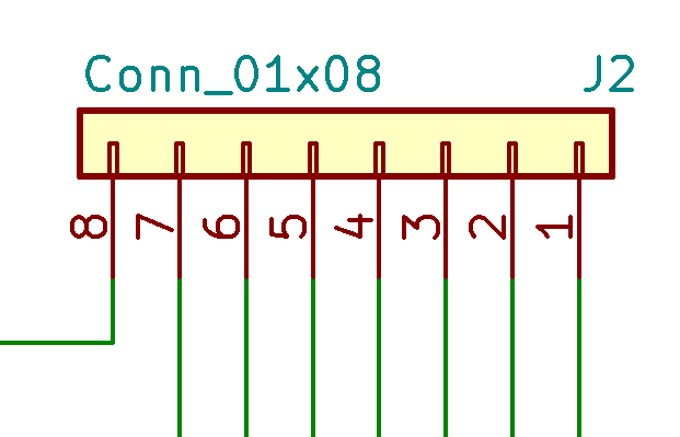
=== J2 - Output Connector === | === J2 - Output Connector === | ||
Revision as of 18:57, 26 November 2021
Contents
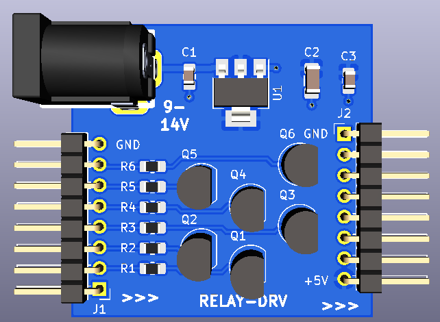
Features
- Inputs
- 6 channels
- Active-high in to drive relay to on state
- 1K to transistor base
- 2.7mA for 3.3V drive
- 4.3mA for 5V drive
- Outputs
- Open Collector outputs from 2N3904 NPN transistors
- Power
- 9-12V power in
- 5V power out to power relays
- DC jack
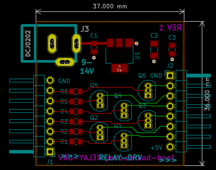
- 36x37mm card
- 3 PCBs for $11 from OshPark
Connectors
J1 - Input Connector
- N/C
- IN1
- IN2
- IN3
- IN4
- IN5
- IN6
- GND
J2 - Output Connector
Power Connector
- Center positive


