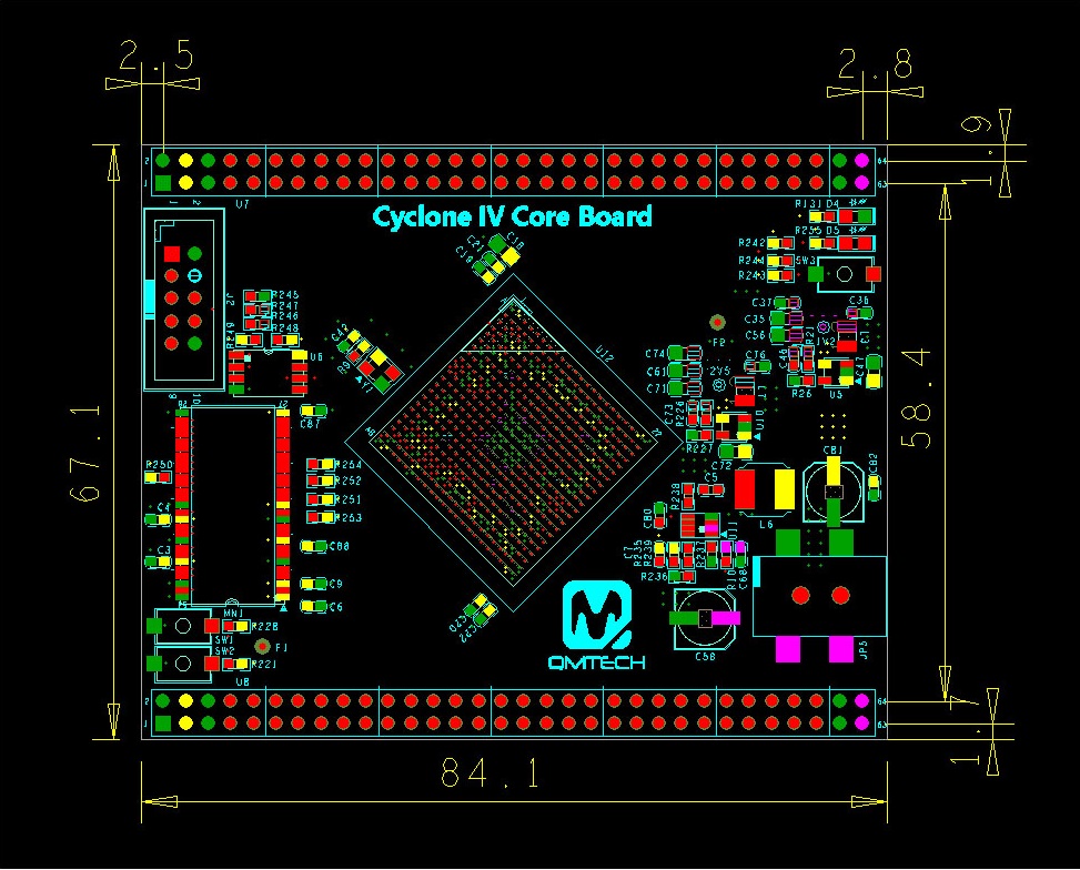
Difference between revisions of "QMTECH EP4CE15 FPGA Card"
Jump to navigation
Jump to search
Blwikiadmin (talk | contribs) |
Blwikiadmin (talk | contribs) |
||
| Line 10: | Line 10: | ||
** DC power jack | ** DC power jack | ||
** Power supply | ** Power supply | ||
| + | |||
| + | == Switches/Indications == | ||
| + | |||
| + | * D4 | ||
| + | * D5 | ||
| + | * SW1 | ||
| + | * SW2 | ||
| + | * SW3 | ||
| + | * JP5 | ||
| + | |||
| + | == Jumpers == | ||
| + | |||
| + | * J2 - JTAG | ||
== Pages == | == Pages == | ||
* [https://github.com/ChinaQMTECH/CYCLONE_IV_EP4CE15 QMTECH EP4CE15] | * [https://github.com/ChinaQMTECH/CYCLONE_IV_EP4CE15 QMTECH EP4CE15] | ||
Revision as of 19:20, 16 January 2020
Contents
Features
- Purchased FPGA Card
- QMTECH EP4CE15 Board
- Altera Cyclone IV EP4CE15F23C8N FPGA
- Winbond W9825C6KH-6 4M X 4 Banks x 16 bits SDRAM
- 3 Switches
- DC power jack
- Power supply
Switches/Indications
- D4
- D5
- SW1
- SW2
- SW3
- JP5
Jumpers
- J2 - JTAG
