Difference between revisions of "ER-PROTO-01"
Jump to navigation
Jump to search
Blwikiadmin (talk | contribs) |
Blwikiadmin (talk | contribs) |
||
| Line 254: | Line 254: | ||
==== Schematic ==== | ==== Schematic ==== | ||
| + | |||
| + | * Opamp buffers | ||
[[file:ER-PROTO-01-CV4_Opamps.PNG]] | [[file:ER-PROTO-01-CV4_Opamps.PNG]] | ||
Revision as of 09:01, 9 November 2022
Features
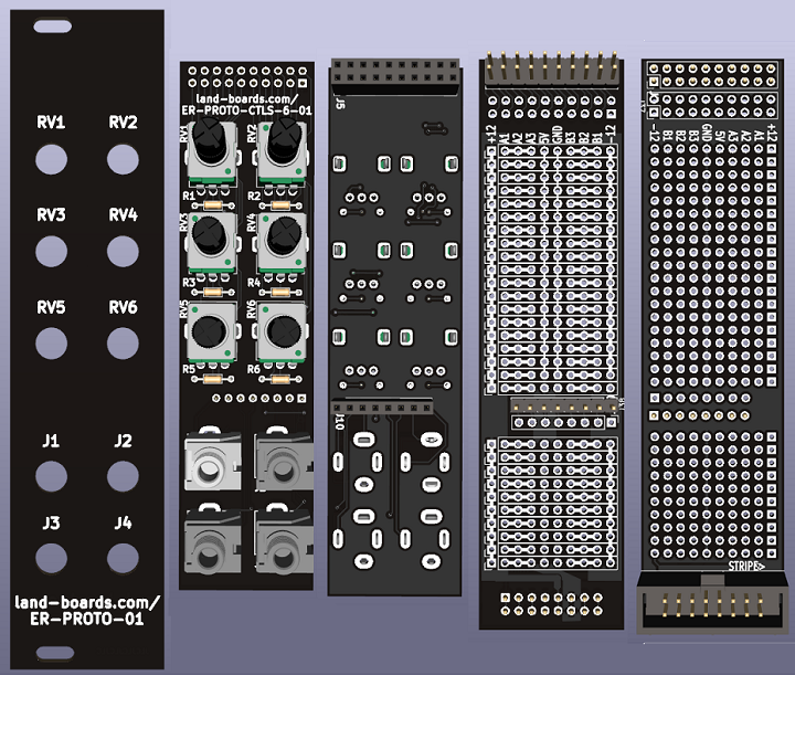
- Eurorack Prototyping card set
- 6 HP wide (30mm) front panel
- 3U tall
- Three card set
- Board interconnect headers duplicated on headers
- 30mm wide front panel
- 28mm wide panel and daughtercards
- 6 POTS
- Marked as RV1-RV5
- Series resistors on pot wiper
- All 3 pot pins brought to top header
- 4 Jacks
- Marked as J1-J4
- Tip/sleeve brought to header near middle/bottom
- Pots on top, jacks on bottom of card
- Easier to adjust pots without bumping into pots
- Pots more often accessed than jacks
- Large prototyping area
- 58 nodes with 3 holes per node (29 per "side")
- +12V, -12V down board edges
- 5V/GND down center of card
- Bussed connections horizontally
- Front Panel with generic labels
- Cover with White on Black P-Touch labels
Connectors
- J1-J4 are front panel connectors
Inter-card Connectors
Pots
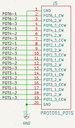
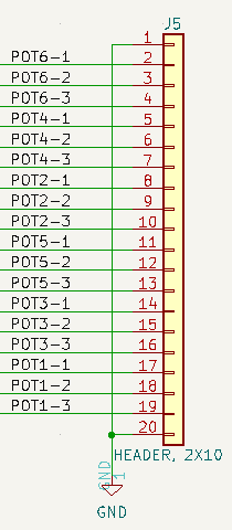
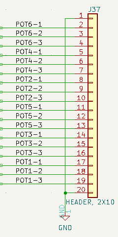
- J5 on the Controls card and J5 on the I/O card
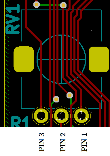
- Pot connections
- POTx-1 is fully CW connects to wiper
- POTx-2 is wiper
- POTX-3 is fully CCW connects to wiper
- To make pot into voltage control
- POTx-1 (CW) = +5V
- POTx-13CCW = GND
- Wire RV1-1 to RV3-1 to RV5-1 on controls card
- Wire RV1-3 to RV3-3 to RV5-3 on controls card
- Wire RV2-1 to RV4-1 to RV6-1 on controls card
- Wire RV2-3 to RV4-3 to RV6-3 on controls card
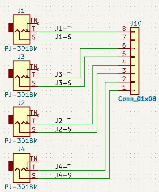
Jacks
- J6 on the controls card and J37 on the I/O card
Daughtercard Connectors
J5, J37 - POT connectione
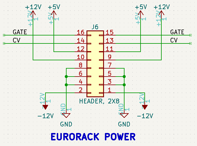
J6 - Eurorack Power
- J6 on the I/O card
- Eurorack power
- 2x5 IDC
- GATE, CV not connected
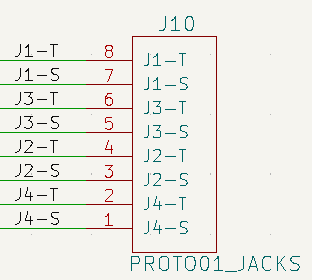
J10 - Jacks connections on Controls card
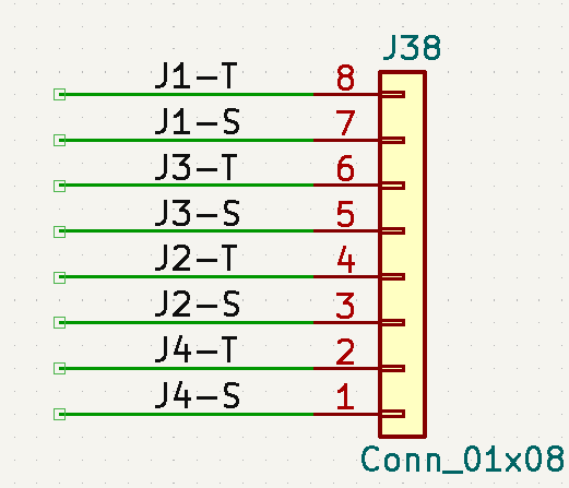
J38 - Jacks connections
Examples
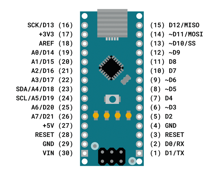
Arduino NANO MOZZI
NANO Pinout
Controls
- 6 Pots
- RV1 = Analog 7
- RV2 - Analog 4
- RV3 - Analog 6
- RV4 - Analog 3
- RV5 - Analog 5
- RV6 - Analog 2
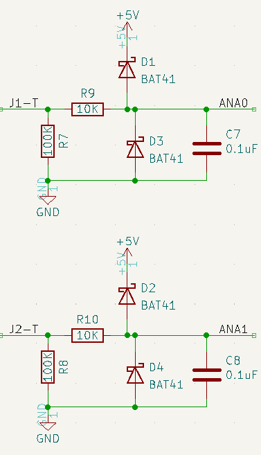
- 2 CV Input Jacks
- J1 = Analog 0
- J2 = Analog 1
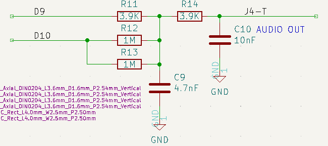
- 1 Output Jack
- J4 = MOZZI HI DEF Audio
Audio Out Schematic
CV In Schematic
- ANA0 in example
Parts
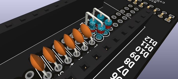
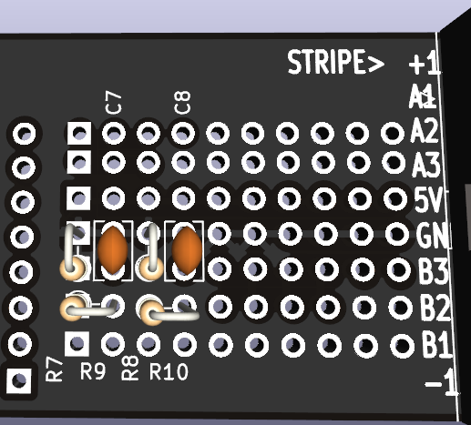
- 3D view
- Top parts view
- Bottom parts view
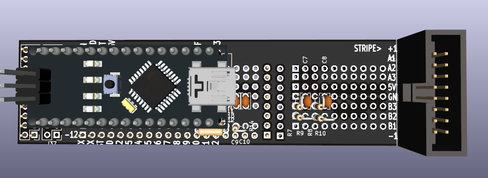
- With NANO
- CAD placement
Wires
NET: ANA0, A1-19, (C7-1, D1-2, D3-1, R9-2)
NET: ANA1, A1-20, (C8-1, D2-2, D4-1, R10-2)
NET: ANA2, A1-21, J37-3
NET: ANA3, A1-22, J37-6
NET: ANA4, A1-23, J37-9
NET: ANA5, A1-24, J37-12
NET: ANA6, A1-25, J37-15
NET: ANA7, A1-26, J37-18
NET: J1-T, J38-1, (R7-1, R9-1)
NET: J2-T, J38-5, (R10-1, R8-1)
NET: J4-T, J38-7, (C10-1, R14-2)
NET: GND1, J37-7
NET: GND2, J38-6
NET: GND3, A1-4
NET: GND4, A1-29
NET: +5VD, A1-27, J37-11
NET: L5V, J37-14, J37-8
NET: LGND, J37-16, J37-4
Parts List
| Find | Qty | Ref Des | Part Number |
|---|---|---|---|
| 1 | 2 | R7, R8 | 100K |
| 2 | 2 | R9, R10 | 10K |
| 3 | 2 | R11, R14 | 3.9K |
| 4 | 2 | R12, R13 | 1M |
| 5 | 4 | D1-D4 | BAT41 |
| 6 | 8 | C1-C8 | 0.1uF |
| 7 | 1 | C9 | 4.7nF |
| 8 | 1 | C10 | 10nF |
| 9 | 1 | J5 | HEADER, 2X10 |
| 10 | 1 | J6 | HEADER, 2X8 |
| 11 | 1 | J10 | HEADER, 1x8 |
| 12 | 1 | A1 | Arduino_Nano_v3 |
Software
- PROTO01_POTS_CHECK.ino - Dump pots/input jacks to screen
CV4 - 4 Control Voltages
- (4) Buffered Outputs
- 4 Pots
- 4 Jacks
- Voltage Levels are assignable via jumpers
- +5V/GND
- +12V/-12V
- +12V/GND
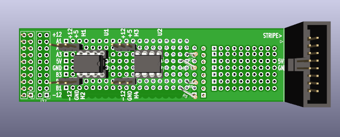
3D PCB Layout
- Board soldermask is actually black, but shown in green for contrast
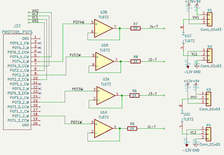
Schematic
- Opamp buffers
