BBB-GVS
Contents
- 1 Beaglebone Black cape which provides 5V GVS connections
- 2 Features
- 3 Technical Overview
- 4 What is GVS?
- 5 The Design
- 6 EEPROM connections
- 7 Beaglebone Black GVS Board Layout
- 8 Connectors
- 9 Analog Port Mapping
- 10 Design Validation Testing
- 11 Production Testing
- 12 Drivers / Example Code
- 13 Assembly Sheet/Parts List
Beaglebone Black cape which provides 5V GVS connections
We love the Beaglebone Black. With all of its I/O connections it offers exciting potential for embedded/connected devices. It even has real mounting holes which let the board be used for real-world applications.
When we got our first Beaglebone Black we were excited to try it with some of our Arduino GVS (Ground/Voltage/Signal) sensors and GVS output devices but couldn't since they are all 5V sensors. Sure we could cobble together some level shifters on a breadboard but in the end we wouldn't have something that could be deployed in a real application What we really wanted was a 5V Sensor shield like the one we use for our Arduino. But there were none out there. So we designed one.
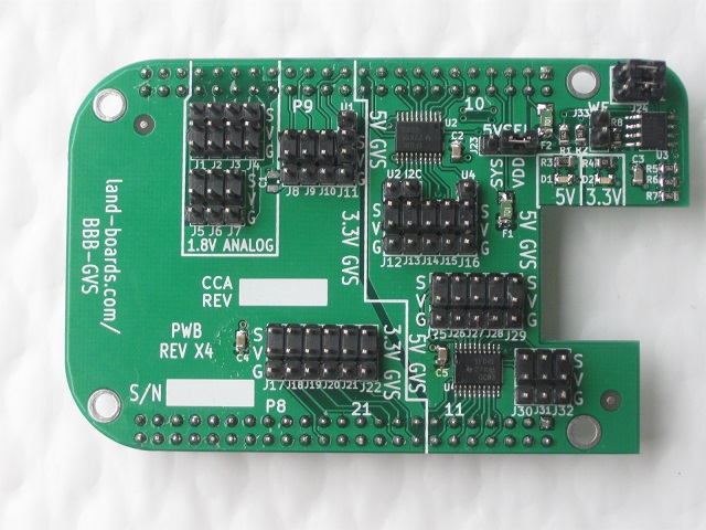
Introducing the BBB-GVS cape.
Features
- (5) 5V GPIO GVS connections (auto direction detection)
- (4) 5V GPIO/Timer GVS connections (auto direction detection)
- (2) 5V UART Tx/Rx connections (auto direction detection)
- (1) 5V PWM GVS connection
- (1) 5V I2C bus 4-pin connections (auto direction detection)
- 5V pins are all ESD protected pins with 15 kV of protection
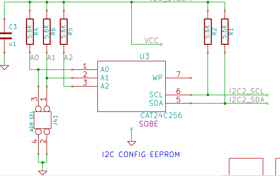
- Cape configuration EEPROM
- (7) 3.3V GPIO connections
- (1) 3.3V UART Tx/Rx connection
- (1) 3.3V PWM GVS connection
- (7) 1.8V analog GVS connections
- Resettable Fuses on 5V and 3.3V power
- Selectable 5V source
- 3.3V and 5V power status LEDs
- Beaglebone Black form factor
Technical Overview
In a nutshell, the 3.3V digital signals of the Beaglebone Black need to be changed into 5V digital signals. There are a number of discrete ways to convert 3.3V bus to 5V signals. Some of them use MOSFETs and a couple of resistors. These work OK but there are some powerful chips out there that can do the conversion even better. We looked around and found what we think is the best 3.3V<>5V data conversion chip, Texas Instrument's TXS0108. The TXS0108 is an 8-bit, bi-directional buffer with automatic direction detection. Each and every pin can transmit and receive independently and even at the same time. The part supports both open drain and push-pull operation. The part can run as fast as 60 Mb/s in push-pull operation and 2 Mb/s in open drain. This speed is fast enough enough for microprocessor GPIO pin or even the fastest serial interfaces that a microprocessor can throw at it.
What is GVS?
GVS is great for prototyping or deploy-able products. The beauty of the GVS connection is that power and ground are provided with each I/O signal. That provides the power needed to power external sensors and output devices. Otherwise splitting the one or two power pins into separate cables ends up being a real mess.
GVS stands for Ground, Voltage and Signal. It's a 3-pin unofficial standard. It uses 0.1" pitch pins. There are a large number of GVS sensors (inputs) and devices (output) parts on ebay. The sorts of GVS sensors include:
- Buttons
- Switches
- Temperature sensors
The sorts of GVS output devices include:
- Relay modules (not always wired as GVS, but they typically require 5V).
- Buzzers
- Solenoids
- Servos (require PWM output pin)
To connect a GVS sensor to a GVS card, just use a 3-wire cable.
Other Connections
The Beaglebone Black also has I2C and UART connections. These allow various devices to be connected:
- I2C Displays
- I2C accelerometers, gyroscopes
- UART GPS modules
The Design
We wanted a sensor shield like the ones use for the Arduino. In the Arduino's case, there's a limited amount of I/O lines The Beaglebone has many more I/O lines than the Arduino. We wanted to convert as many of the signals to 5V as we could possible fit on a board the size of a mint can. In particular, we wanted to convert the I2C bus as well as the UART lines to 5V. Also, we wanted to have a mix of 3.3V and 5V GVS signals. We also wanted to allow external connection to the analog inputs as we providing the analog reference voltage to run the analog input sensors.
That translated into 2 parts which handle 8 I/O lines each. Putting these parts along with all the GVS connections we could possibly add resulted in our design.
Voltage Translators
The BBB-GVS board uses Texas Instrument TXS0108 voltage translators.
Voltage Translators Features
- No Direction-Control Signal Needed
- Max Data Rates
- 60 Mbps (Push Pull)
- 2 Mbps (Open Drain)
- 1.2 V to 3.6 V on A Port and 1.65 V to 5.5 V on
- B Port (VCCA ≤ VCCB)
- No Power-Supply Sequencing Required –
- Either VCCA or VCCB Can Be Ramped First
- Latch-Up Performance Exceeds 100 mA Per JESD 78, Class II
- ESD Protection Exceeds JESD 22 (A Port)
- 2000-V Human-Body Model (A114-B)
- 150-V Machine Model (A115-A)
- 1000-V Charged-Device Model (C101)
- IEC 61000-4-2 ESD (B Port)
- ±6-kV Air-Gap Discharge
- ±8-kV Contact Discharge
Voltage Translators Architecture
The TXS0108E can be used in level-translation applications for interfacing devices or systems operating at different interface voltages with one another. The TXS0108E is ideal for use in applications where an open-drain driver is connected to the data I/Os. The TXS0108E can also be used in applications where a push-pull driver is connected to the data I/Os, but the TXB0104 might be a better option for such push-pull applications. The TXS0108E device is a semi-buffered auto-direction-sensing voltage translator design is optimized for translation applications (e.g. MMC Card Interfaces) that require the system to start out in a low-speed open-drain mode and then switch to a higher speed push-pull mode.
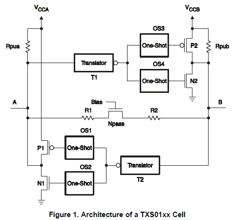
To address these application requirements, a semi-buffered architecture design is used and is illustrated above (see Figure 1). Edge-rate accelerator circuitry (for both the high-to-low and low-to-high edges), a High-Ron n-channel pass-gate transistor (on the order of 300 Ω to 500 Ω) and pull-up resistors (to provide DC-bias and drive capabilities) are included to realize this solution. A direction-control signal (to control the direction of data flow from A to B or from B to A) is not needed. The resulting implementation supports both low-speed open-drain operation as well as high-speed push-pull operation.
When transmitting data from A to B ports, during a rising edge the One-Shot (OS3) turns on the PMOS transistor (P2) for a short-duration and this speeds up the low-to-high transition. Similarly, during a falling edge, when transmitting data from A to B, the One-Shot (OS4) turns on NMOS transistor (N2) for a short-duration and this speeds up the high-to-low transition. The B-port edge-rate accelerator consists of one-shots OS3 and OS4, Transistors P2 and N2 and serves to rapidly force the B port high or low when a corresponding transition is detected on the A port.
When transmitting data from B to A ports, during a rising edge the One-Shot (OS1) turns on the PMOS transistor (P1) for a short-duration and this speeds up the low-to-high transition. Similarly, during a falling edge, when transmitting data from B to A, the One-Shot (OS2) turns on NMOS transistor (N1) for a short-duration and this speeds up the high-to-low transition. The A-port edge-rate accelerator consists of one-shots OS1 and OS2, Transistors P1 and N1 components and form the edge-rate accelerator and serves to rapidly force the A port high or low when a corresponding transition is detected on the B port.
EEPROM connections
Beaglebone Black GVS Board Layout
Connectors
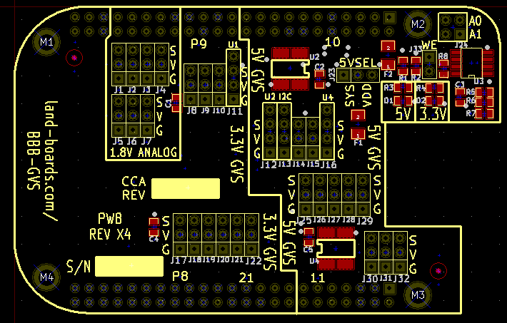
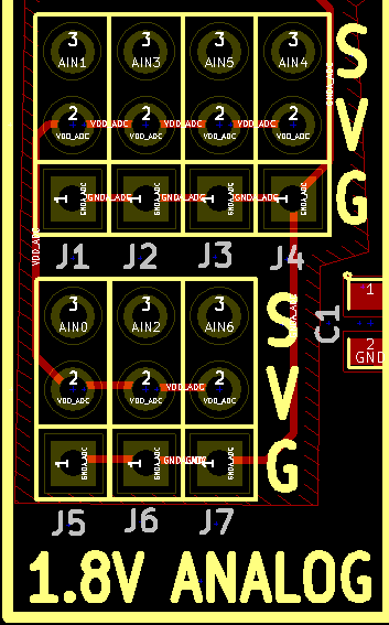
J1-J7 Analog Inputs
- Analog signals must be between 0 and 1.8V/
J1-J7 pin 1 = P9-34 = GND_ADC

J1-J7 pin 2 = P9-32 = BDD_ADC

Connector	Pin	Function
J1-3	P9_40	AIN1
J2-3	P9_38	AIN3
J3-3	P9_36	AIN5
J4-3	P9_33	AIN4
J5-3	P9_39	AIN0
J6-3	P9_37	AIN2
J7-3	P9_35	AIN6
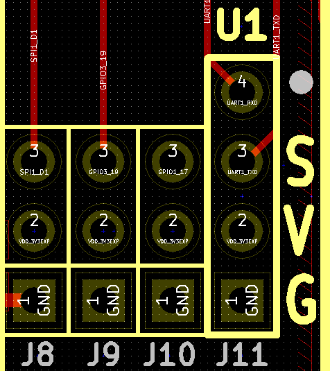
J8-J11 GPIO, UART1 - 3.3V
- 3.3V digital
Connector	Pin	Function	GPIO
J8-3	P9_30	SPI_D1	GPIO3_16
J9-3	P9_27	GPIO3_19	GPIO3_19
J10-3	P9_23	GPIO1_17	GPIO1_17
J11-3	P9_24	UART1_TXD	GPIO0_15
J11-4	P9_26	UART1_RXD	GPIO0_14
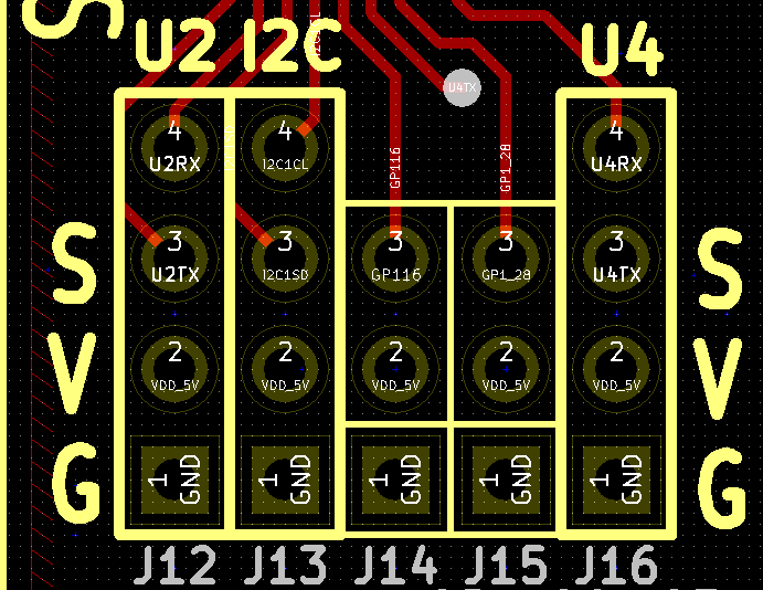
J12-J16 - UART2, I2C1, GPIOs, UART4 - 5V
- 5V digital
Connector	Pin	Function	GPIO
J12-3	P9_21	UART2TX	GPIO0_3
J12-4	P9_22	UART2RX	GPIO0_2
J13-3	P9_18	I2C1SDA	GPIO0_12
J13-4	P9_17	I2C1SCL	GPIO0_13
J14-3	P9_15	GPIO1_16	GPIO1_16
J15-3	P9_12	GPIO1_28	GPIO1_28
J16-3	P9_13	UART4TX	GPIO0_31
J16-4	P9_11	UART4RX	GPIO0_30
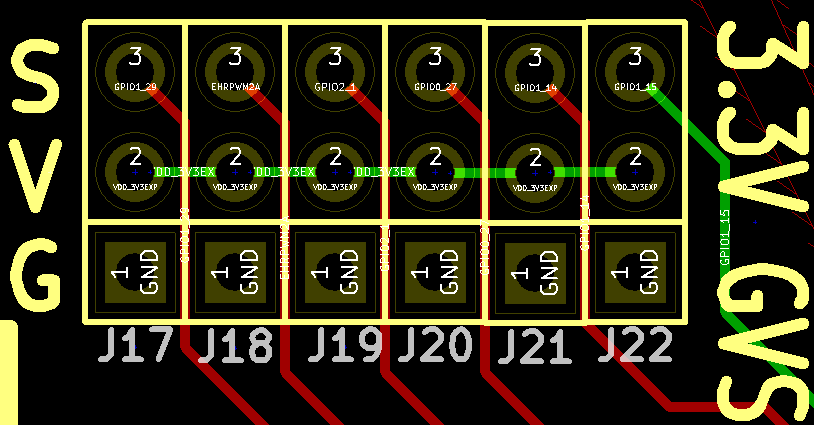
J17-J22 GPIOs, PWM2A, 3.3V
- 3.3V digital
Connector	Pin	Function	GPIO
J17-3	P8_26	GPIO1_29	GPIO1_29
J18-3	P8_19	EHRPWM2A	GPIO0_22
J19-3	P8_18	GPIO2_1	GPIO2_1
J20-3	P8_17	GP1O0_27	GPIO0_27
J21-3	P8_16	GPIO1_14	GPIO1_14
J22-3	P8_15	GPIO1_15	GPIO1_15
J23 - 5VSEL
Jumper 1-2 to power BBB-GVS board from SYS_5V. (default)
Jumper 2-3 to power board from VDD_5V. VDD_5V is 5V with a maximum current of 1000mA, but only works if the BeagleBone is powered by an external power source
BBB-GVS-X3-J23.PNG
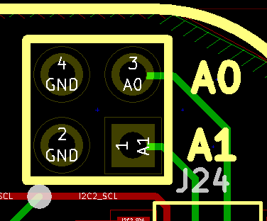
J24 - EEPROM address selection jumpers
EEPROM address A0, A1 selection jumper selectable.
Default = both installed.
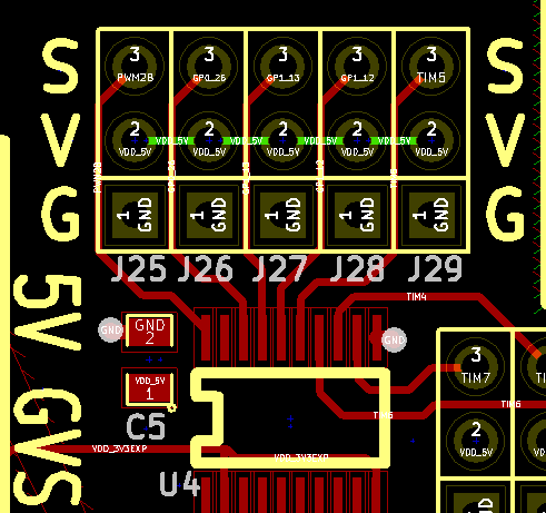
J25-J29 PWM2B, GPIOs, TIMERs - 5V
5V digital
Connector	Pin	Function	GPIO
J25-3	P8_13	EHRPWM2B	GPIO0_23
J26-3	P8_14	GPIO0_26	GPIO0_26
J27-3	P8_11	GPIO1_13	GPIO1_13
J28-3	P8_12	GPIO1_12	GPIO1_12
J29-3	P8_9	TIMER5	GPIO2_5
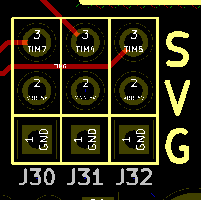
J30-J32 - TIMERs - 5V
5V digital
Connector	Pin	Function	GPIO
J30-3	P8_8	TIMER7	GPIO2_3
J31-3	P8_7	TIMER4	GPIO1_3
J32-3	P8_10	TIMER6	GPIO2_4
J33 - EEPROM Write Enable
Install jumper to enable writes. Remove jumper to disable writes (default).
Analog Port Mapping
Connector	Pin	Function	Alternate	Voltage
J1-3	P9_40	AIN1		1.8V Analog
J2-3	P9_38	AIN3		1.8V Analog
J3-3	P9_36	AIN5		1.8V Analog
J4-3	P9_33	AIN4		1.8V Analog
J5-3	P9_39	AIN0		1.8V Analog
J6-3	P9_37	AIN2		1.8V Analog
J7-3	P9_35	AIN6		1.8V Analog
Python Analog and Digital Pin Definitions by Header J Number
J1 = "AIN1"
J2 = "AIN3"
J3 = "AIN5"
J4 = "AIN4"
J5 = "AIN0"
J6 = "AIN2"
J7 = "AIN6"
J8 = "P9_30"
J9 = "P9_27"
J10 = "P9_23"
J11_3 = "P9_24"
J11_4 = "P9_26"
J12_3 = "P9_21"
J12_4 = "P9_22"
J13_3 = "P9_18"
J13_4 = "P9_17"
J14 = "P9_15"
J15 = "P9_12"
J16_3 = "P9_13"
J16_4 = "P9_11"
J17 = "P8_26"
J18 = "P8_19"
J19 = "P8_18"
J20 = "P8_17"
J21 = "P8_16"
J22 = "P8_15"
J25 = "P8_13"
J26 = "P8_14"
J27 = "P8_11"
J28 = "P8_12"
J29 = "P8_9"
J30 = "P8_8"
J31 = "P8_7"
J32 = "P8_10"
Design Validation Testing
I2C Testing
Here are the steps we followed to test the I2C bus on the BBB-GVS.
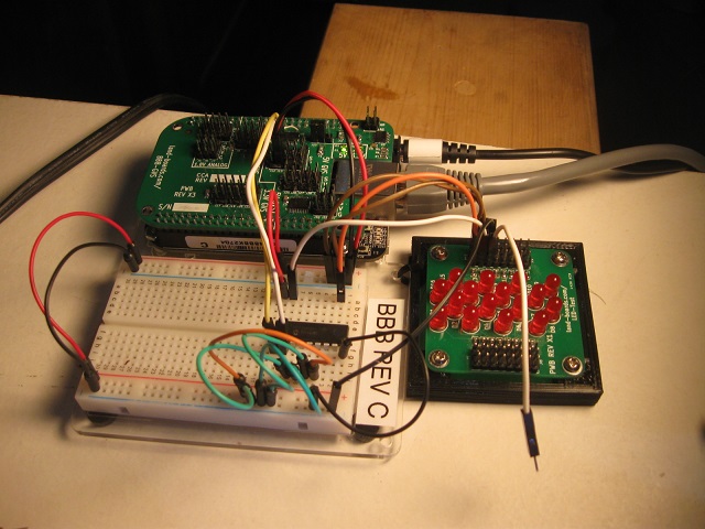
Hook up a MCP23008 I2C Port expander
- Hook up
- Running on BBB-GVS so we can run the MCP23008 at 5V
- Using LED-Test card as LEDs
- Running on Rev C h/w with Debian o/s (page did not list the o/s)
- Running 'sudo apt-get install i2c-tools' showed that i2c-tools was already installed
- Command 'i2cdetect -r -y 3' returns error
root@beaglebone:~# i2cdetect -r -y 3
Error: Could not open file `/dev/i2c-3' or `/dev/i2c/3': No such file or directory
- Is this because the '3' is wrong?
- SPOILER ALERT - The '3' is wrong but there were other things wrong
Mapping I2c busses
From https://groups.google.com/forum/#!msg/beagleboard/v9r8UkN7klk/h3rFKFJDLnUJ
- i2c-1 is the enumeration linux gave one of the i2c buses and does not necessarily correspond to the i2c pins you are using.
- The BBB has two usable i2c devices [1], as follows:
- i2c0: Not exposed in the expansion headers
- i2c1: pins P9 17,18 (and 24,26)
- i2c2: pins P9 19,20 (and 21,22)
- The i2c devices appear in the AM335x memory map [2] at the following locations:
- i2c0: 0x44E0_B000
- i2c1: 0x4802_A000
- i2c2: 0x4819_C000
- This is what we see when I enter
ls -l /dev/i2c*
- Returns
crw-rw---T 1 root i2c 89, 0 Apr 23 16:46 /dev/i2c-0
crw-rw---T 1 root i2c 89, 1 Apr 23 16:46 /dev/i2c-1
root@beaglebone:~# ls -l /sys/bus/i2c/devices/i2c-*
lrwxrwxrwx 1 root root 0 Apr 23 16:46 /sys/bus/i2c/devices/i2c-0 -> ../../../devices/ocp.3/44e0b000.i2c/i2c-0
lrwxrwxrwx 1 root root 0 Apr 23 16:46 /sys/bus/i2c/devices/i2c-1 -> ../../../devices/ocp.3/4819c000.i2c/i2c-1
- So it looks from the addresses like the I2C1 port is not enabled/exposed...
Enabling I2C1
The page BeagleBone Black I2C References page has one way to enable the I2C
- Enter
echo BB-I2C1 > /sys/devices/bone_capemgr.8/slots
ls -l /sys/bus/i2c/devices/i2c-*
- And, returns
lrwxrwxrwx 1 root root 0 Nov  3 21:49 /sys/bus/i2c/devices/i2c-0 -> ../../../devices/ocp.2/44e0b000.i2c/i2c-0
lrwxrwxrwx 1 root root 0 Nov  3 21:49 /sys/bus/i2c/devices/i2c-1 -> ../../../devices/ocp.2/4819c000.i2c/i2c-1
lrwxrwxrwx 1 root root 0 Nov  3 21:50 /sys/bus/i2c/devices/i2c-2 -> ../../../devices/ocp.2/4802a000.i2c/i2c-2
- Our number was not .8 which we found by
root@beaglebone:~# ls /sys/devices
44e10800.pinmux  breakpoint         ocp.3     soc.1     tracepoint
ARMv7 Cortex-A8  fixedregulator.10  platform  software  virtual
bone_capemgr.9   iio_sysfs_trigger  pmu.0     system
- We typed:
root@beaglebone:~# echo BB-I2C1 > /sys/devices/bone_capemgr.9/slots
- No error, but did it work?
root@beaglebone:~# ls -l /sys/bus/i2c/devices/i2c-*

lrwxrwxrwx 1 root root 0 Apr 24 02:10 /sys/bus/i2c/devices/i2c-0 -> ../../../devices/ocp.3/44e0b000.i2c/i2c-0
lrwxrwxrwx 1 root root 0 Apr 24 02:10 /sys/bus/i2c/devices/i2c-1 -> ../../../devices/ocp.3/4819c000.i2c/i2c-1
lrwxrwxrwx 1 root root 0 Aug 17 07:29 /sys/bus/i2c/devices/i2c-2 -> ../../../devices/ocp.3/4802a000.i2c/i2c-2
- YES! We can now see the next port
- Testing to see if the MCP23008 part is there:
root@beaglebone:~# i2cdetect -r -y 2
     0  1  2  3  4  5  6  7  8  9  a  b  c  d  e  f
00:          -- -- -- -- -- -- -- -- -- -- -- -- --
10: -- -- -- -- -- -- -- -- -- -- -- -- -- -- -- --
20: 20 -- -- -- -- -- -- -- -- -- -- -- -- -- -- --
30: -- -- -- -- -- -- -- -- -- -- -- -- -- -- -- --
40: -- -- -- -- -- -- -- -- -- -- -- -- -- -- -- --
50: -- -- -- -- -- -- -- -- -- -- -- -- -- -- -- --
60: -- -- -- -- -- -- -- -- -- -- -- -- -- -- -- --
70: -- -- -- -- -- -- -- --
- It does work! The map looks just like it did in the first page
- Not sure why the instructions in the first page indicated that the port is 3?
Back to the MCP23008
http://www.gigamegablog.com/2012/11/04/beaglebone-coding-101-i2c/
- Loading the program
wget http://gigamega-micro.googlecode.com/files/WeatherBone.tgz
tar -xzvf WeatherBone.tgz
cd WeatherBone
python gm-mcp23008.py
- Did not work. File name has underscore, not hyphen.
python gm-mcp23008.py
- Got an error
root@beaglebone:~/WeatherBone# python gm_mcp23008.py
Traceback (most recent call last):
  File "gm_mcp23008.py", line 204, in <module>
    mcp = mcp23008(3, 0x20, True)
  File "gm_mcp23008.py", line 54, in __init__
    self.__i2c = Adafruit_I2C(mcp23008_addr, i2c_busnumber, False)
  File "/root/WeatherBone/Adafruit_I2C.py", line 15, in __init__
    self.bus = smbus.SMBus(busnum)
IOError: [Errno 2] No such file or directory
- Changed
if __name__ == '__main__':
    mcp = mcp23008(3, 0x20, True)
    # button 1 connected to ground on pin 0 of MCP23008
- to
if __name__ == '__main__':
    mcp = mcp23008(2, 0x20, True)
    # button 1 connected to ground on pin 0 of MCP23008
- Message
root@beaglebone:~/WeatherBone# python gm_mcp23008.py
ERROR: Interrupts not supported on output pin
ERROR: Interrupts not supported on output pin
- It worked
- Taking pin 10 of the MCP23008 low resulted in the light blinking
- This shows read/write of I2C1 works through the BBB-GVS
- https://www.youtube.com/watch?v=IipxhRRkrz8
Testing Configuration I2C EEPROM
- BBB I2C EEPROM programming
- EEPROM programming
- From the previous steps...
root@beaglebone:~/WeatherBone# ls -l /sys/bus/i2c/devices/i2c-*
lrwxrwxrwx 1 root root 0 Apr 24 02:10 /sys/bus/i2c/devices/i2c-0 -> ../../../devices/ocp.3/44e0b000.i2c/i2c-0
lrwxrwxrwx 1 root root 0 Apr 24 02:10 /sys/bus/i2c/devices/i2c-1 -> ../../../devices/ocp.3/4819c000.i2c/i2c-1
lrwxrwxrwx 1 root root 0 Aug 17 07:29 /sys/bus/i2c/devices/i2c-2 -> ../../../devices/ocp.3/4802a000.i2c/i2c-2
- 4819c000.i2c/i2c-1 is I2C2. Confusing, huh?
root@beaglebone:~/WeatherBone# i2cdetect -r -y 1
     0  1  2  3  4  5  6  7  8  9  a  b  c  d  e  f
00:          -- -- -- -- -- -- -- -- -- -- -- -- --
10: -- -- -- -- -- -- -- -- -- -- -- -- -- -- -- --
20: -- -- -- -- -- -- -- -- -- -- -- -- -- -- -- --
30: -- -- -- -- -- -- -- -- -- -- -- -- -- -- -- --
40: -- -- -- -- -- -- -- -- -- -- -- -- -- -- -- --
50: -- -- -- -- UU UU UU UU -- -- -- -- -- -- -- --
60: -- -- -- -- -- -- -- -- -- -- -- -- -- -- -- --
70: -- -- -- -- -- -- -- --
- This page says that UU means the device is busy.
- Tried this:
root@beaglebone:~# dmesg | grep at24
[    0.575927] at24 0-0050: 32768 byte 24c256 EEPROM, writable, 1 bytes/write
[    0.575974] at24 1-0054: 32768 byte 24c256 EEPROM, writable, 1 bytes/write
[    0.576014] at24 1-0055: 32768 byte 24c256 EEPROM, writable, 1 bytes/write
[    0.576053] at24 1-0056: 32768 byte 24c256 EEPROM, writable, 1 bytes/write
[    0.576091] at24 1-0057: 32768 byte 24c256 EEPROM, writable, 1 bytes/write
- That is good. From what I can tell the driver is ready for an EEPROM at address 0x54.
- The Configuration EEPROM on the BBB-GVS is at address 0x54.
- But is it really "there"?
root@beaglebone:~# cat /sys/bus/i2c/devices/1-0054/eeprom | hexdump -C
00000000  ff ff ff ff ff ff ff ff  ff ff ff ff ff ff ff ff  |................|
- That is also good. It shows that the part is at 0x54 and is unprogrammed.
- But how to tell it's just not a false response?
- Try the next address.
root@beaglebone:~# cat /sys/bus/i2c/devices/1-0055/eeprom | hexdump -C
cat: /sys/bus/i2c/devices/1-0055/eeprom: Connection timed out
- That is good. It shows that no part is at 0x55.
- Removing the A0 jumper gets this:
root@beaglebone:~# cat /sys/bus/i2c/devices/1-0055/eeprom | hexdump -C
00000000  ff ff ff ff ff ff ff ff  ff ff ff ff ff ff ff ff  |................|
root@beaglebone:~# cat /sys/bus/i2c/devices/1-0054/eeprom | hexdump -C
cat: /sys/bus/i2c/devices/1-0054/eeprom: Connection timed out
- Looks like reads are working
- These are the elements associated with the EEPROM:
root@beaglebone:~# ls /sys/bus/i2c/devices/1-0054/
driver  eeprom  modalias  name  power  subsystem  uevent
- Now to test writes...
root@beaglebone:~# echo "Hello Kickstarter supporters." > /sys/bus/i2c/devices/1-0054/eeprom
root@beaglebone:~# cat /sys/bus/i2c/devices/1-0054/eeprom | hexdump -C
00000000  48 65 6c 6c 6f 20 4b 69  63 6b 73 74 61 72 74 65  |Hello Kickstarte|
00000010  72 20 73 75 70 70 6f 72  74 65 72 73 2e 0a ff ff  |r supporters....|
00000020  ff ff ff ff ff ff ff ff  ff ff ff ff ff ff ff ff  |................|
- Working!!!
Setting up the Configuration EEPROM
- Used the mkeeprom tool to create a data.eeprom file.
root@beaglebone:~/BBB/mkeeprom# cat data.eeprom > /sys/bus/i2c/devices/1-0054/eeprom
Dumping the EEPROM
root@beaglebone:~/BBB/mkeeprom# cat /sys/bus/i2c/devices/1-0054/eeprom | hexdump -C
00000000  aa 55 33 ee 41 30 42 42  42 2d 47 56 53 00 00 00  |.U3.A0BBB-GVS...|
00000010  00 00 00 00 00 00 00 00  00 00 00 00 00 00 00 00  |................|
00000020  00 00 00 00 00 00 58 33  00 00 6c 61 6e 64 2d 62  |......X3..land-b|
00000030  6f 61 72 64 73 2e 63 6f  6d 00 42 42 42 2d 47 56  |oards.com.BBB-GV|
00000040  53 00 00 00 00 00 00 00  00 00 00 02 30 30 30 30  |S...........0000|
00000050  30 31 00 00 00 00 00 00  00 00 00 00 00 00 00 00  |01..............|
00000060  00 00 00 00 00 00 00 00  00 00 00 00 00 00 00 00  |................|
*
000000d0  00 00 00 00 00 00 00 00  e0 18 00 00 00 00 00 00  |................|
000000e0  a0 28 00 00 00 00 00 00  00 00 00 00 00 64 00 64  |.(...........d.d|
000000f0  00 64 00 00 ff ff ff ff  ff ff ff ff ff ff ff ff  |.d..............|
00000100  ff ff ff ff ff ff ff ff  ff ff ff ff ff ff ff ff  |................|
Production Testing
Setup
- Install BBB-GVS on BBB
- Install shunt at J23-1 to -2 (SYS on 5VSEL)
- Install shunts at A0 and A1
- Install shunt at J33 WE
- Ethernet connection to BBB
- Power via 5V jack to BBB
- Must power card with wall wart - can't use USB 5V adapter
- Verify 5V and 3.3V LEDs are lit
- Log in via putty
- User = root
- Password = enter
Analog Testing
- Connect GRID49 card with resistor ladder
- (8) 10K resistors
- From 1.8V to all 7 inputs to ground
- Input in 1/8 steps
- A12 marked on cable connector goes to A12 on GRID49 board
- Extra wire goes to J12 pin on GRID49 board
- Run analog ladder code
cd ~/pyBBB/BBB-GVS-3/analogLadder
python analogLadder.py
- Pass/Fail message will be displayed
- Approximate expected values are
val0  0.625
val1  0.125
val2  0.750
val3  0.250
val4  0.500
val5  0.375
val6  0.875
PASS - Analog values match expected ladder values
GPIO Testing
- Hook up LED-32 Card to these pins
D0 = "P9_30"
D16 = "P9_27"
D1 = "P9_23"
D17 = "P9_24"
D2 = "P9_26"
D18 = "P9_21"
D3 = "P9_22"
D19 = "P9_18"
D4 = "P9_17"
D20 = "P9_15"
D5 = "P9_12"
D21 = "P9_13"
D6 = "P9_11"
D22 = "P8_26"
D7 = "P8_19"
D23 = "P8_18"
D8 = "P8_17"
D24 = "P8_16"
D9 = "P8_15"
D25 = "P8_13"
D10 = "P8_14"
D11 = "P8_12"
D26 = "P8_11"
D27 = "P8_9"
D12 = "P8_8"
D28 = "P8_7"
D13 = "P8_10"
cd /root/BBB/BBB-GVS/blink-BBB-GVS/src
python blink-BBB-GVS.py
- LEDs should light for all channels
- D5, D19 stay lit during the test
- Disconnect cables
I2C Testing/EEPROM Programming
- A0, A1 address jumpers should be installed
- Go to directory
- Program the EEPROM via
- Verify by typing
cd ~/BBB/mkeeprom
cat data.eeprom > /sys/bus/i2c/devices/1-0054/eeprom
cat /sys/bus/i2c/devices/1-0054/eeprom | hexdump -C
- Result should be like -
00000000  aa 55 33 ee 41 30 42 42  42 2d 47 56 53 00 00 00  |.U3.A0BBB-GVS...|
00000010  00 00 00 00 00 00 00 00  00 00 00 00 00 00 00 00  |................|
00000020  00 00 00 00 00 00 58 33  00 00 6c 61 6e 64 2d 62  |......X3..land-b|
00000030  6f 61 72 64 73 2e 63 6f  6d 00 42 42 42 2d 47 56  |oards.com.BBB-GV|
00000040  53 00 00 00 00 00 00 00  00 00 00 02 30 30 30 30  |S...........0000|
00000050  30 31 00 00 00 00 00 00  00 00 00 00 00 00 00 00  |01..............|
00000060  00 00 00 00 00 00 00 00  00 00 00 00 00 00 00 00  |................|
- Remove WE jumper
- Type
cat data.eeprom > /sys/bus/i2c/devices/1-0054/eeprom
Result should be error
root@beaglebone:~/BBB/mkeeprom# cat data.eeprom > /sys/bus/i2c/devices/1-0054/eeprom
cat: write error: Connection timed out
- Prepare to re-run
- Type
halt

