KiCad
Contents
Notes on Running KiCad
Some misc. stuff
Custom BOM Python Script (KiCad 6)
- Create a BOM that requires minimal manual editing to use on MediaWiki webpage
- Adds Datasheet path to Description
- Creates BOM .csv file in the folder where the schematic is located
Source Code
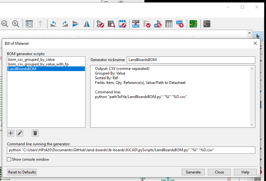
- LandBoardsBOM.py - our BOM script that runs from "Generate Bill of Materials..." in KiCad Schematic Editor
- Based on com_csv_grouped_by_value.py that comes in KiCad 6
- Also requires files from the KiCad installation (get latest from the KiCad installation folder)
- Put the 3 scripts into folder in KiCad projects pyScripts folder
Running
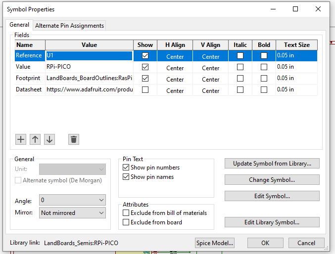
- Add links to schematic parts
- Run BOM tool inside schematic
- Add link to script in KiCad
- Click Generate
Post-Processing
- Edit in spreadsheet program
- Use pyCSVtoMWTable to create MediaWiki format output
Panelizing
GerberPanelizer Steps in KiCad 6
- Make card
- Run/resolve all DRCs in PCB
- Set Place > Grid Origin to upper left corner of board
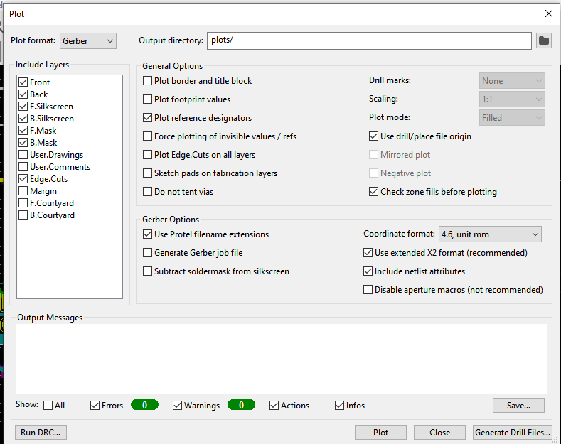
- Gerbers
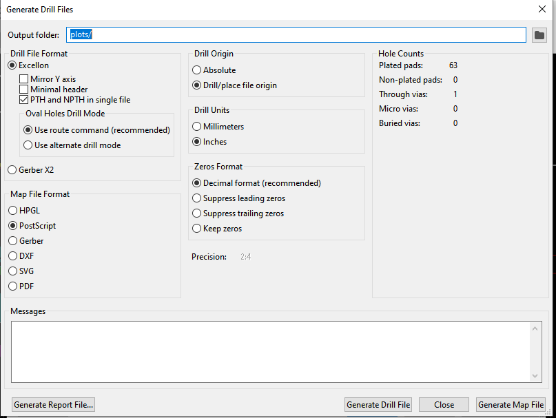
- Use auxiliary axis as origin
- Protel extensions
- Save Drill file
- Rename EdgeCuts .gm1 file to .gko
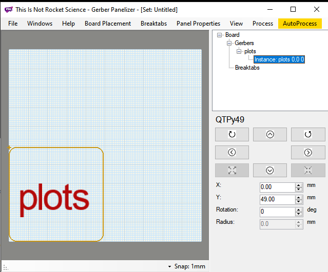
- Run GerberPanelizer
- File > New
- Select board placement → add gerber folder
- File browser is painful (can't easily browse)
- Library > Documents > GitHub > land-boards > lb-boards > folder_with_gerbers
- File browser is painful (can't easily browse)
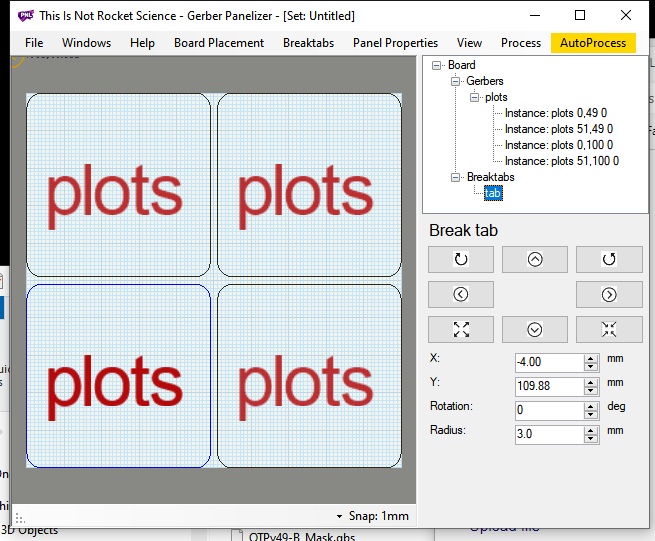
- Board Placement > Autopack: Naive
- Select Board instance in upper right box
- Right click, Add instance
- Repeat for all boards
- Board Placement > Autopack: Naive
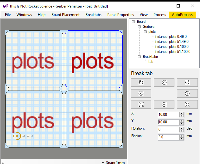
- Breaktabs < Insert Breaktab
- If not visible, change numbers to 10, 10
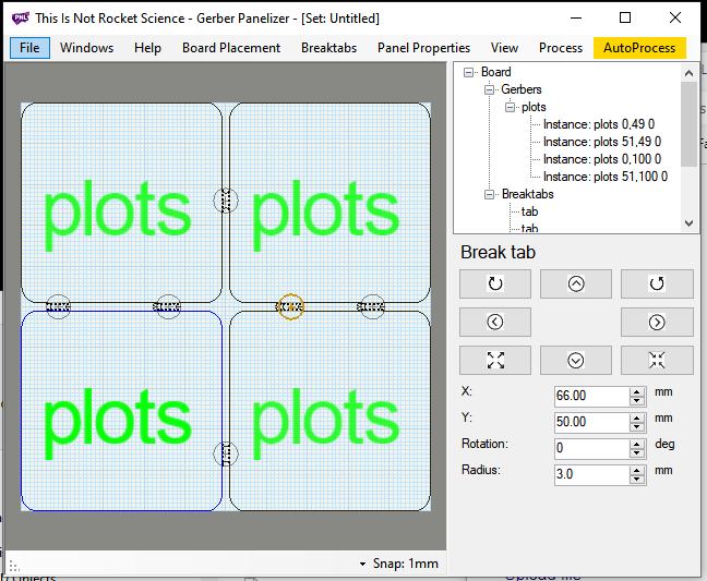
- Manually move to spot
- Repeat until cards are all green
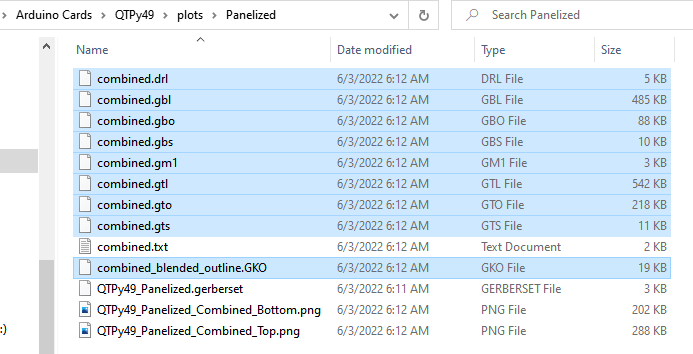
- file → save as to panel folder
- file → export merged file
- Painful browser to planelized folder
- Make zip
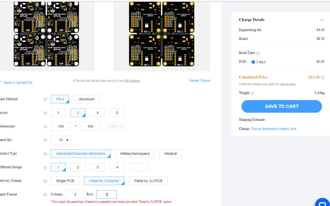
- Ordering on jlcpcb
- Upload file
- Select qty, color
- Select panel by customer
- Enter array dimensions
- Ignore error?
- Not cost goes from $5 to $12.30 for qty 10
SPICE Simulation
Create Footprints Using FreeCAD
- Our very simple example
"Standard" Footprints
- KiCad footprints can be a pain so this documents the footprints we commonly use
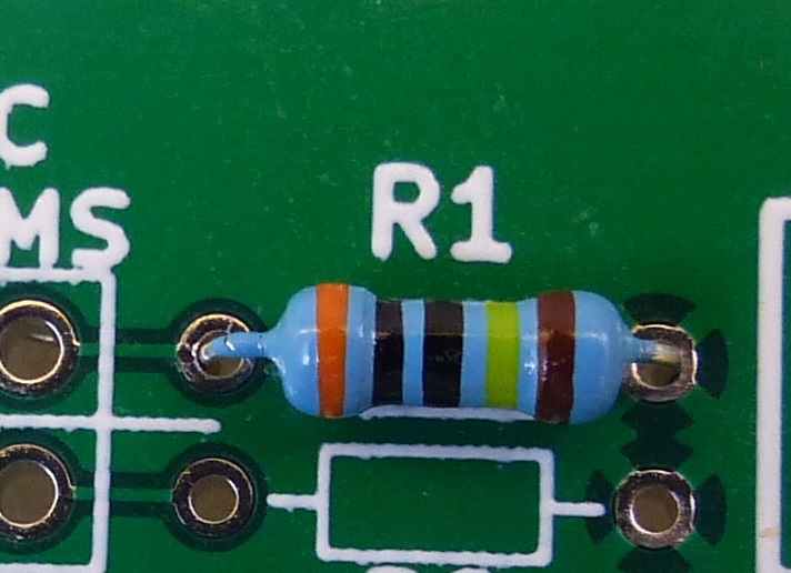
1/8 W resistor footprint
- Part on PCB
- KiCad v6 footprint
Resistor_THT:R_Axial_DIN0204_L3.6mm_D1.6mm_P7.62mm_Horizontal
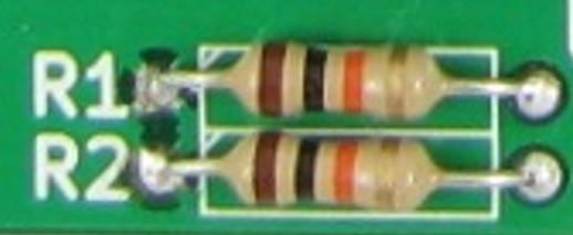
- Also fits 1/4W resistors with leads bent straight down
1/4 W resistor footprint
- Part on PCB
- KiCad v6 footprint
Resistor_THT:R_Axial_DIN0207_L6.3mm_D2.5mm_P10.16mm_Horizontal
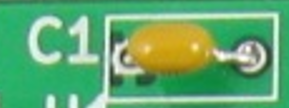
Cap, 0.2" pitch
- Part on PCB
- KiCad v6 footprint
Capacitor_THT:C_Rect_L7.0mm_W3.5mm_P5.00mm
D-Sub Connectors
DB-25F
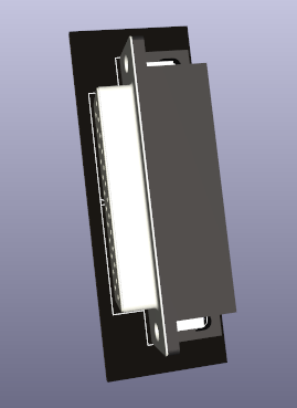
- D25S33E4PA00LF - DB-25F
- 3D part
- ${KICAD6_3DMODEL_DIR}/Connector_Dsub.3dshapes/DSUB-25_Female_Horizontal_P2.77x2.84mm_EdgePinOffset7.70mm_Housed_MountingHolesOffset9.12mm.wrl
- Schematic symbol
- LandBoards_Conns:DB25FC_Oval_Pads
Board Design Templates
- KiCad Templates for
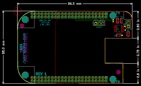
- BeagleBone Black Capes
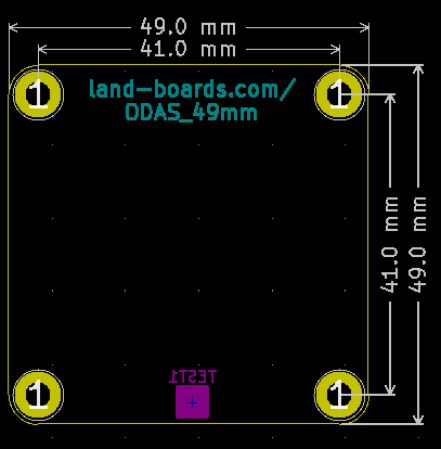
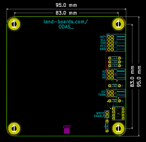
- ODAS 49mm Cards
- ODAS 95mm Cards
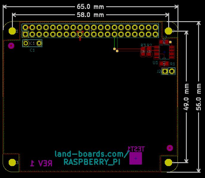
- Raspberry Pi Plus Hats
- Templates Repository
- ZIP files of each template inside each folder
