Difference between pages "File:RF-Amp W2AEW S11 1-30MHz.png" and "RF-Amp"
(Difference between pages)
Jump to navigation
Jump to search
Blwikiadmin (talk | contribs) (Blwikiadmin uploaded a new version of File:RF-Amp W2AEW S11 1-30MHz.png) |
Blwikiadmin (talk | contribs) |
||
| Line 1: | Line 1: | ||
| + | [[File:RF-Amp_P1943-720px.jpg]] | ||
| + | == RF Amplifier Features == | ||
| + | |||
| + | * Useful as an IF or Antenna Amplifier | ||
| + | * From [https://zl2ctm.blogspot.com/2020/11/go-qrp-portable-ssb-rig.html Charlie Morris' (ZL2CTM) Go QRP Portable SSB Rig] | ||
| + | ** Charlie references Solid State Design for the Radio Amateur (pp 19-20) | ||
| + | * Single 2N3904 NPN transistor | ||
| + | ** Ft = 300 MHz (Gain Bandwidth Product) | ||
| + | *** Theoretical gain | ||
| + | **** +20 dB at 30 MHz | ||
| + | **** +29.5 dB at 10 MHz | ||
| + | **** Reality is lower due to capacitance, etc. | ||
| + | * Measured +22 dB gain @12V, +25dB gain @14V | ||
| + | * Input connectors: SMA or BNC | ||
| + | * +12V nominal power | ||
| + | * 49x49mm card | ||
| + | * 4x 4-40 mounting holes | ||
| + | |||
| + | == RF Amplifier Design == | ||
| + | |||
| + | === Schematic === | ||
| + | |||
| + | [[file:RF_Amp_Schematic-4.PNG]] | ||
| + | |||
| + | == LT Spice Simulation == | ||
| + | |||
| + | * [https://github.com/land-boards/lb-boards/blob/master/HamRadio/RF-Amp/LTSpice/2n3904%20amp.asc LTspice Simulation] - GitHub source file | ||
| + | ** +28.4 dB at 9 MHz | ||
| + | |||
| + | [[File:RF-AMP-LTSPICE_XFMRS.PNG]] | ||
| + | |||
| + | == Charlie Morris Design == | ||
| + | |||
| + | * From Charlie's notes with mods for my use | ||
| + | ** [https://zl2ctm.blogspot.com/2020/11/go-qrp-portable-ssb-rig.html Charlie Morris' (ZL2CTM) Go QRP Portable SSB Rig] | ||
| + | ** Charlie describes the design in detail in his video [https://www.youtube.com/watch?v=CHdtoupH2Vg Simple SSB Rig: Part 6 - IF Amplifiers] (Feb 2021) | ||
| + | ** Based on the Class A RF Amplifier in [https://www.amazon.com/Solid-State-Design-Radio-Amateur/dp/0872590402 Solid State Design for the Radio Amateur] pp 19-20 | ||
| + | * [https://www.mouser.com/datasheet/2/308/1/2N3903_D-2310199.pdf 2N3904 data sheet] | ||
| + | * [https://www.electronics-tutorials.ws/amplifier/emitter-resistance.html Emitter Resistance] - helpful paper | ||
| + | |||
| + | === Beta DC === | ||
| + | |||
| + | * Geometric mean min/max beta at operating current | ||
| + | ** =sqrt(100*300) = 173 | ||
| + | |||
| + | === Beta AC === | ||
| + | |||
| + | * Gain bandwidth product divided by operating frequency | ||
| + | ** Assume operating frequency of 9 MHz (IF frequency) | ||
| + | ** = 300/9 = 33.3 | ||
| + | |||
| + | === DC Operating Point === | ||
| + | |||
| + | * Max HFE RF gain at CE current of 10 mA | ||
| + | ** If Vce = 6V, this is 60 mW power dissipation | ||
| + | * Assume Ve (voltage across emitter resistor) = 1/10 Vcc = 12V/10 = 1.2V | ||
| + | ** R3 is Re (emitter resistor) = 1.2V/0.01A = 120 ohms | ||
| + | * VCE = 0.7V (typical from data sheet) | ||
| + | * V(emitter) at 10% of Vcc rule of thumb = 1.2V | ||
| + | * V(base) = V(emitter) + VCE = 1.9V | ||
| + | * Base current is collector current divided by Beta DC | ||
| + | ** Biasing resistors = 10x current needed by base current | ||
| + | ** 10 mA in C-E, beta DC less = 10 mA/173 = 58 uA | ||
| + | ** 10x the current in the biasing resistors = 580 uA (calculated) | ||
| + | * R2 is 1.9V at 580 uA = 3.29K use 3.3K | ||
| + | * R1 sources current to R2 and transistor base | ||
| + | ** Voltage = Vcc (12V) - 1.9V = 10.1V | ||
| + | ** Current = 577 uA + 58 uA = 635 uA | ||
| + | ** R1 = 10.1 / .635 mA = 15.9K, use 15K | ||
| + | |||
| + | ==== Measured DC operating point ==== | ||
| + | |||
| + | * Measured with no input | ||
| + | * Vcc = 11.96V | ||
| + | * Current draw = 12 mA | ||
| + | ** Quick test for wiring and more or less correct parts | ||
| + | ** Expected 11 mA - close enough | ||
| + | * +BUFF = 11.84V | ||
| + | ** 0.12V which is 12 mA through R4 10 ohms - expected | ||
| + | * V emitter = 1.41V | ||
| + | ** 1.41V/12 Ohms = 11.75 mA close to 12 mA total measured current | ||
| + | * V on input divider = 2.06V | ||
| + | ** Vbase + 0.7V - close | ||
| + | ** Measured Vbe = 2.06-1.41 = 0.65 - close | ||
| + | |||
| + | === Input resistance === | ||
| + | |||
| + | * Xc for 0.1uF cap from emitter to ground | ||
| + | ** C=0.1uF | ||
| + | ** F=10MHz | ||
| + | ** 1/2*pi*F*C = 0.16 ohms | ||
| + | * Parallel resistors R1, R2 paralleled with transistor input impedance | ||
| + | ** R1=15K, R2=3.3K | ||
| + | ** Transistor resistance = Beta AC (33.3) times re | ||
| + | *** re = 26 / Ie (10 mA in mA) = 26/10 = 2.6 | ||
| + | *** SSDRA uses 25 as constant - close enough | ||
| + | **** 26 comes from Ebers-Moll approximation | ||
| + | *** Beta AC * re = 33.3*2.6 = 83.3 ohms - predominates | ||
| + | ** All in parallel are 80.8 ohms | ||
| + | |||
| + | === Gain calculation === | ||
| + | |||
| + | * Approximation | ||
| + | * Ic = 0.01A | ||
| + | * Rc = 200 | ||
| + | * Vrc = 2V | ||
| + | * Gain = Vrc / vt | ||
| + | ** vt = 26 mV at room temperature | ||
| + | ** Gain = 2V / .026V = 79.2 V/V | ||
| + | ** Gain = +37 dB | ||
| + | |||
| + | === Input/Output Transformers === | ||
| + | |||
| + | * Using [http://toroids.info/FT37-43.php FT37-43 Toroid] | ||
| + | |||
| + | [[file:FT37-43_10_Turns.PNG]] | ||
| + | |||
| + | ==== Tracks ==== | ||
| + | |||
| + | [[file:RF-Amp-tracks.PNG]] | ||
| + | |||
| + | ==== Input Transformer ==== | ||
| + | |||
| + | * Input Transformer (T1 on Charlie's - T2 on this board) | ||
| + | * Need to calculate turns ratio | ||
| + | * 50:80.8 Ohms | ||
| + | * n = sqrt(Zout/Zin)sqrt(80.8/50) = 1.27 turns ratio | ||
| + | * Turns choices | ||
| + | * Minimum number of turns | ||
| + | * Rule of thumb - want Xl (coil impedance smallest value) to be least 4-5X the load | ||
| + | ** Load = 80.8 ohms | ||
| + | ** 5 * 80.8 ohms = 404.2 ohms minimum | ||
| + | *** More turns = larger capacitance and drops bandwidth | ||
| + | ** Toroid is FT37-43 | ||
| + | ** From [http://toroids.info/FT37-43.php Toroid page] | ||
| + | *** Xl = 404.4 at 9 MHz is 4.5 turns, round up to 5 | ||
| + | ** Try nearest integer numbers turns ratios | ||
| + | *** 5:6 = 6% error | ||
| + | *** 6:8 = -4.6% | ||
| + | *** 7:9 = -1.1% << good choice | ||
| + | *** 8:10 = +1.7% | ||
| + | *** 9:11 = +4.0% | ||
| + | *** 10:13 = -2.19% | ||
| + | * Use 7:9 turns ratio for optimal input transformer | ||
| + | |||
| + | [[file:RF-Amp-T2.PNG]] | ||
| + | |||
| + | ==== Output Transformer ==== | ||
| + | |||
| + | * Output transformer (T2 on Charlie's - T1 on this board) | ||
| + | * T2 - different than Charlie's design since my Crystal filters are all 50 ohms in/out | ||
| + | * SSDRA suggest presenting 200 ohm load to the collector | ||
| + | ** Can't find reference in SSDRA | ||
| + | ** Reflecting back 50 ohms load to 200 ohm collector... | ||
| + | * 200:50 ohms | ||
| + | * n = sqrt(200/50) = 2.0:1 turns ratio | ||
| + | * 10:5 turns | ||
| + | ** 10 turns primary (on transistor collector) | ||
| + | *** 10 turns = 35 uH | ||
| + | ** 5 turns secondary (towards output) | ||
| + | *** 5 turns = 8.75 uH | ||
| + | ** 15 turns = 9.5 in | ||
| + | |||
| + | [[file:RF-Amp-T1.PNG]] | ||
| + | |||
| + | === Charlie's Notes === | ||
| + | |||
| + | [[FILE:IF Amp_0046A.jpg]] | ||
| + | |||
| + | [[FILE:IF Amp_0046B.jpg]] | ||
| + | |||
| + | [[FILE:IF Amp_0046C.jpg]] | ||
| + | |||
| + | [[FILE:IF Amp_0047A.jpg]] | ||
| + | |||
| + | [[FILE:IF Amp_0047B.jpg]] | ||
| + | |||
| + | [[FILE:IF Amp_0047C.jpg]] | ||
| + | |||
| + | == NanoVNA Measurements == | ||
| + | |||
| + | * '''Goal''': Measure RF-Amp performance using a [[NanoVNA]] running [https://nanovna.com/?page_id=90 NanoSaver software on PC] | ||
| + | * S21 (gain) needs to be measured with a [[RF_Attenuators#40_dB_Attenuator|40 dB attenuator]] on input to RF-Amp to avoid compression on the output | ||
| + | * S11 (reflection) input impedance can't be measured with input [[RF_Attenuators#40_dB_Attenuator|40 dB attenuator]] because S11 just ends up measuring the attenuator | ||
| + | ** Output should be terminated to 50 ohms for S11 measurement | ||
| + | * DC current = 12 mA | ||
| + | |||
| + | === Measure S21 === | ||
| + | |||
| + | * Put [[RF_Attenuators#40_dB_Attenuator|40 dB attenuator]] on RF-Amp input, measure S21 at output | ||
| + | ** [[NanoVNA]] provides 50 ohm load to RF-Amp to properly terminate output | ||
| + | * Measure S21 with 9:11 input transformer | ||
| + | ** S21 @ 100 KHz = -8 dB dB | ||
| + | ** S21 @ 1.45 MHz = 35.4 dB (peak gain) | ||
| + | ** S21 @ 9.1 MHz = 24.3 dB | ||
| + | ** S21 @ 16 MHz = 20.1 dB | ||
| + | ** S21 @ 30 MHz = 12.7 dB | ||
| + | * Peak gain justifies use of 40 dB attenuator to protect [[NanoVNA]] | ||
| + | |||
| + | [[file:RF-Amp_S21_40dBAttenInput_1-30MHz.png]] | ||
| + | |||
| + | ==== LTspice vs NanoVNA ==== | ||
| + | |||
| + | * LTspice simulation was pretty similar to [[NanoVNA]] results | ||
| + | ** -10 dB at 100 KHz | ||
| + | ** +32 dB at peak | ||
| + | ** Lower output at higher frequencies | ||
| + | |||
| + | [[file:RF-Amp_S21_LTspice-vs-NanoVNA_1-30MHz.png]] | ||
| + | |||
| + | === Measure Input Compression === | ||
| + | |||
| + | * Is there compression if the [[NanoVNA]] drives the input directly? | ||
| + | ** Test by driving directly from NanoVNA set to CW = 9 MHz | ||
| + | ** Measured output with scope - not clipped at 9 MHz | ||
| + | *** Approx. 1Vpp input = +22.1 dBm gain which matches the S21 with the attenuator on the input | ||
| + | *** Vpp = 12.4V with 50 Ohm load resistor | ||
| + | ** Starts clipping at 7 Mhz and down | ||
| + | * Therefore, can measure input impedance at 9 MHz | ||
| + | * Other evidence of compression | ||
| + | ** Compare S21 gain with no input attenuator, put external [[RF Attenuators|40 dB RF Attenuators]] on output of RF-Amp to protect [[NanoVNA]] input | ||
| + | ** S21 shows lower gain in lower frequencies so clipping/compression is happening | ||
| + | ** Was: 35 dB at 1.4 MHz | ||
| + | ** Is: 23.1 dB at 1.5 MHz | ||
| + | * Due to compression can't accurately measure lower frequencies with attenuator at output | ||
| + | * Compression below 7 MHz matches what was on scope | ||
| + | |||
| + | [[file:RF-Amp_S21_40dBAttenOutput_1-30MHz.png]] | ||
| + | |||
| + | === Measure Input Impedance === | ||
| + | |||
| + | * Shows VSWR at 14.4 MHz = 1.56:1 | ||
| + | * At 9 MHz | ||
| + | ** VSWR = 1.7:1 | ||
| + | ** Impedance = 81-j10 | ||
| + | |||
| + | [[file:RF-Amp_AttenOutput_VSWR_2021_1-30MHz.png]] | ||
| + | |||
| + | === Change Input Transformer turns ratio === | ||
| + | |||
| + | * Above had 9:11 turns ratio | ||
| + | * Change to 7:9 turns ratio | ||
| + | * Slightly better gain at higher frequencies | ||
| + | * Was: S21 @ 30 MHz = 12.7 dB | ||
| + | * After: S21 @ 30 MHz = 15.3 dB | ||
| + | * Small additional gain at 8 MHz | ||
| + | ** Was: S21 @ 9.1 MHz = 24.3 dB | ||
| + | ** After: S21 @ 9.1 MHz = 24.8 dB | ||
| + | |||
| + | [[file:RF-Amp_S21_40dBAttenInput_Turns7to9_1-30MHz.png]] | ||
| + | |||
| + | * New turns improved the input VSWR slightly | ||
| + | * Was: At 9 MHz, VSWR = 1.7:1, Impedance = 81-j10 | ||
| + | * After: At 9 MHz, VSWR = 1.6:1, Impedance = 76.7-j12 | ||
| + | |||
| + | [[file:RF-Amp_vswr_40dBAttenInput_Turns7to9_1-30MHz.png]] | ||
| + | |||
| + | ==== Tune input transformer==== | ||
| + | |||
| + | * Isolate output by replacing output transformer with 200 resistor | ||
| + | * Add one more output winding to input transformer T2 (7:10) | ||
| + | * VSWR nearly 1.04:1 at 11.1 MHz | ||
| + | * -19 dB return loss at 9 MHz VSWR = 1.249:1 | ||
| + | |||
| + | [[file:RF-Amp_VSWR_1-30MHz_7to10Turns.png]] | ||
| + | |||
| + | * With output transformer | ||
| + | * Slightly better with 1 extra winding | ||
| + | |||
| + | [[file:RF-Amp_VSWR_1-30MHz_7to10Turns-2.png]] | ||
| + | |||
| + | == W2AEW Measurement Method == | ||
| + | |||
| + | * See [https://youtu.be/7TtKE39TWpI W2AEW #337 video] below | ||
| + | * Insert 30 dB attenuator and calibrate with attenuator installed | ||
| + | * Open/sort/thru at the output side of the attenuator using [[NanoVNA#RF_Demo_Kit|NanoVNA RF Demo Kit]] | ||
| + | * Scan 1-30 Mhz | ||
| + | ** Overdriven at 1 MHz | ||
| + | * Re-calibrate at 1.5-31.5 MHz | ||
| + | * 9 MHz measurement | ||
| + | ** VSWR = 1.172 | ||
| + | ** S11 (Return Loss) = -22.014 dB | ||
| + | ** S21 (Gain) = +23.624 dB | ||
| + | |||
| + | [[file:RF-Amp_W2AEW_S21_1-30MHz.png]] | ||
| + | |||
| + | [[file:RF-Amp_W2AEW_S11_1-30MHz.png]] | ||
| + | |||
| + | == Video == | ||
| + | |||
| + | <video type="youtube">7TtKE39TWpI</video> | ||
| + | |||
| + | <video type="youtube">CHdtoupH2Vg</video> | ||
| + | |||
| + | <video type="youtube">YJTsWV2kzFY</video> | ||
| + | |||
| + | <video type="youtube">xPFzFhM0ojE</video> | ||
| + | |||
| + | == Assembly Sheet == | ||
| + | |||
| + | * [[RF Amplifier Assembly Sheet]] | ||
Revision as of 12:16, 13 November 2021

Contents
RF Amplifier Features
- Useful as an IF or Antenna Amplifier
- From Charlie Morris' (ZL2CTM) Go QRP Portable SSB Rig
- Charlie references Solid State Design for the Radio Amateur (pp 19-20)
- Single 2N3904 NPN transistor
- Ft = 300 MHz (Gain Bandwidth Product)
- Theoretical gain
- +20 dB at 30 MHz
- +29.5 dB at 10 MHz
- Reality is lower due to capacitance, etc.
- Theoretical gain
- Ft = 300 MHz (Gain Bandwidth Product)
- Measured +22 dB gain @12V, +25dB gain @14V
- Input connectors: SMA or BNC
- +12V nominal power
- 49x49mm card
- 4x 4-40 mounting holes
RF Amplifier Design
Schematic

LT Spice Simulation
- LTspice Simulation - GitHub source file
- +28.4 dB at 9 MHz

Charlie Morris Design
- From Charlie's notes with mods for my use
- Charlie Morris' (ZL2CTM) Go QRP Portable SSB Rig
- Charlie describes the design in detail in his video Simple SSB Rig: Part 6 - IF Amplifiers (Feb 2021)
- Based on the Class A RF Amplifier in Solid State Design for the Radio Amateur pp 19-20
- 2N3904 data sheet
- Emitter Resistance - helpful paper
Beta DC
- Geometric mean min/max beta at operating current
- =sqrt(100*300) = 173
Beta AC
- Gain bandwidth product divided by operating frequency
- Assume operating frequency of 9 MHz (IF frequency)
- = 300/9 = 33.3
DC Operating Point
- Max HFE RF gain at CE current of 10 mA
- If Vce = 6V, this is 60 mW power dissipation
- Assume Ve (voltage across emitter resistor) = 1/10 Vcc = 12V/10 = 1.2V
- R3 is Re (emitter resistor) = 1.2V/0.01A = 120 ohms
- VCE = 0.7V (typical from data sheet)
- V(emitter) at 10% of Vcc rule of thumb = 1.2V
- V(base) = V(emitter) + VCE = 1.9V
- Base current is collector current divided by Beta DC
- Biasing resistors = 10x current needed by base current
- 10 mA in C-E, beta DC less = 10 mA/173 = 58 uA
- 10x the current in the biasing resistors = 580 uA (calculated)
- R2 is 1.9V at 580 uA = 3.29K use 3.3K
- R1 sources current to R2 and transistor base
- Voltage = Vcc (12V) - 1.9V = 10.1V
- Current = 577 uA + 58 uA = 635 uA
- R1 = 10.1 / .635 mA = 15.9K, use 15K
Measured DC operating point
- Measured with no input
- Vcc = 11.96V
- Current draw = 12 mA
- Quick test for wiring and more or less correct parts
- Expected 11 mA - close enough
- +BUFF = 11.84V
- 0.12V which is 12 mA through R4 10 ohms - expected
- V emitter = 1.41V
- 1.41V/12 Ohms = 11.75 mA close to 12 mA total measured current
- V on input divider = 2.06V
- Vbase + 0.7V - close
- Measured Vbe = 2.06-1.41 = 0.65 - close
Input resistance
- Xc for 0.1uF cap from emitter to ground
- C=0.1uF
- F=10MHz
- 1/2*pi*F*C = 0.16 ohms
- Parallel resistors R1, R2 paralleled with transistor input impedance
- R1=15K, R2=3.3K
- Transistor resistance = Beta AC (33.3) times re
- re = 26 / Ie (10 mA in mA) = 26/10 = 2.6
- SSDRA uses 25 as constant - close enough
- 26 comes from Ebers-Moll approximation
- Beta AC * re = 33.3*2.6 = 83.3 ohms - predominates
- All in parallel are 80.8 ohms
Gain calculation
- Approximation
- Ic = 0.01A
- Rc = 200
- Vrc = 2V
- Gain = Vrc / vt
- vt = 26 mV at room temperature
- Gain = 2V / .026V = 79.2 V/V
- Gain = +37 dB
Input/Output Transformers
- Using FT37-43 Toroid

Tracks

Input Transformer
- Input Transformer (T1 on Charlie's - T2 on this board)
- Need to calculate turns ratio
- 50:80.8 Ohms
- n = sqrt(Zout/Zin)sqrt(80.8/50) = 1.27 turns ratio
- Turns choices
- Minimum number of turns
- Rule of thumb - want Xl (coil impedance smallest value) to be least 4-5X the load
- Load = 80.8 ohms
- 5 * 80.8 ohms = 404.2 ohms minimum
- More turns = larger capacitance and drops bandwidth
- Toroid is FT37-43
- From Toroid page
- Xl = 404.4 at 9 MHz is 4.5 turns, round up to 5
- Try nearest integer numbers turns ratios
- 5:6 = 6% error
- 6:8 = -4.6%
- 7:9 = -1.1% << good choice
- 8:10 = +1.7%
- 9:11 = +4.0%
- 10:13 = -2.19%
- Use 7:9 turns ratio for optimal input transformer

Output Transformer
- Output transformer (T2 on Charlie's - T1 on this board)
- T2 - different than Charlie's design since my Crystal filters are all 50 ohms in/out
- SSDRA suggest presenting 200 ohm load to the collector
- Can't find reference in SSDRA
- Reflecting back 50 ohms load to 200 ohm collector...
- 200:50 ohms
- n = sqrt(200/50) = 2.0:1 turns ratio
- 10:5 turns
- 10 turns primary (on transistor collector)
- 10 turns = 35 uH
- 5 turns secondary (towards output)
- 5 turns = 8.75 uH
- 15 turns = 9.5 in
- 10 turns primary (on transistor collector)

Charlie's Notes


NanoVNA Measurements
- Goal: Measure RF-Amp performance using a NanoVNA running NanoSaver software on PC
- S21 (gain) needs to be measured with a 40 dB attenuator on input to RF-Amp to avoid compression on the output
- S11 (reflection) input impedance can't be measured with input 40 dB attenuator because S11 just ends up measuring the attenuator
- Output should be terminated to 50 ohms for S11 measurement
- DC current = 12 mA
Measure S21
- Put 40 dB attenuator on RF-Amp input, measure S21 at output
- NanoVNA provides 50 ohm load to RF-Amp to properly terminate output
- Measure S21 with 9:11 input transformer
- S21 @ 100 KHz = -8 dB dB
- S21 @ 1.45 MHz = 35.4 dB (peak gain)
- S21 @ 9.1 MHz = 24.3 dB
- S21 @ 16 MHz = 20.1 dB
- S21 @ 30 MHz = 12.7 dB
- Peak gain justifies use of 40 dB attenuator to protect NanoVNA

LTspice vs NanoVNA
- LTspice simulation was pretty similar to NanoVNA results
- -10 dB at 100 KHz
- +32 dB at peak
- Lower output at higher frequencies

Measure Input Compression
- Is there compression if the NanoVNA drives the input directly?
- Test by driving directly from NanoVNA set to CW = 9 MHz
- Measured output with scope - not clipped at 9 MHz
- Approx. 1Vpp input = +22.1 dBm gain which matches the S21 with the attenuator on the input
- Vpp = 12.4V with 50 Ohm load resistor
- Starts clipping at 7 Mhz and down
- Therefore, can measure input impedance at 9 MHz
- Other evidence of compression
- Compare S21 gain with no input attenuator, put external 40 dB RF Attenuators on output of RF-Amp to protect NanoVNA input
- S21 shows lower gain in lower frequencies so clipping/compression is happening
- Was: 35 dB at 1.4 MHz
- Is: 23.1 dB at 1.5 MHz
- Due to compression can't accurately measure lower frequencies with attenuator at output
- Compression below 7 MHz matches what was on scope

Measure Input Impedance
- Shows VSWR at 14.4 MHz = 1.56:1
- At 9 MHz
- VSWR = 1.7:1
- Impedance = 81-j10

Change Input Transformer turns ratio
- Above had 9:11 turns ratio
- Change to 7:9 turns ratio
- Slightly better gain at higher frequencies
- Was: S21 @ 30 MHz = 12.7 dB
- After: S21 @ 30 MHz = 15.3 dB
- Small additional gain at 8 MHz
- Was: S21 @ 9.1 MHz = 24.3 dB
- After: S21 @ 9.1 MHz = 24.8 dB

- New turns improved the input VSWR slightly
- Was: At 9 MHz, VSWR = 1.7:1, Impedance = 81-j10
- After: At 9 MHz, VSWR = 1.6:1, Impedance = 76.7-j12

Tune input transformer
- Isolate output by replacing output transformer with 200 resistor
- Add one more output winding to input transformer T2 (7:10)
- VSWR nearly 1.04:1 at 11.1 MHz
- -19 dB return loss at 9 MHz VSWR = 1.249:1

- With output transformer
- Slightly better with 1 extra winding

W2AEW Measurement Method
- See W2AEW #337 video below
- Insert 30 dB attenuator and calibrate with attenuator installed
- Open/sort/thru at the output side of the attenuator using NanoVNA RF Demo Kit
- Scan 1-30 Mhz
- Overdriven at 1 MHz
- Re-calibrate at 1.5-31.5 MHz
- 9 MHz measurement
- VSWR = 1.172
- S11 (Return Loss) = -22.014 dB
- S21 (Gain) = +23.624 dB


Video
Assembly Sheet
File history
Click on a date/time to view the file as it appeared at that time.
| Date/Time | Thumbnail | Dimensions | User | Comment | |
|---|---|---|---|---|---|
| current | 12:07, 13 November 2021 | 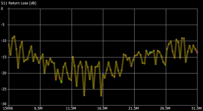 | 694 × 381 (11 KB) | Blwikiadmin (talk | contribs) |
You cannot overwrite this file.
File usage
The following page uses this file: