IntegTheremin

Features
The Integrated Theremin combines five of our boards into one. The boards included are:
- MiniDuino
- 16 MHz ATMega 328 processor
- Arduino UNO Code and IDE Compatible
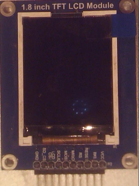
- TFT Display connector
- FTDI-USB-TTL
- USB Interface
- Board is not powerable from FTDI
- HV Digital Pots
- 10-bits, 1024 steps
- Control Frequency and Voltage
- AudioAmp386
- 3/4 Watt Output
- Standard RCA phone style connector
- XR-2206 Voltage Controlled Oscillator
- Waveform Adjustment pot from X3 version of XR-2206
Additional Features
The board has additional features including:
- Advanced Power Supply Design
- Single +12V power supply input
- +5V High-Efficiency Switcher to drive logic and High Intensity IR Sensors
- Previous (separate board) design had a hot regulator on the MiniDuino
- Due to the current drop of the +12V or +9V to 5V
- At 200 mA due to the IR sensor cards
- Due to the current drop of the +12V or +9V to 5V
- Previous (separate board) design had a hot regulator on the MiniDuino
- Total power Measured at 12V, 130 mA = 1.6 Watts
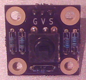
- Dedicated connectors for IR Sensors
- Direct (DC) coupling for Voltage Controlled Oscillator to Audio Amplifier
- AC cap in series with the previous design led to clipping of the audio
- Added connection to allow Microprocessor to monitor (via A/D) the VCO level for smoother volume control transitions
- Write all of the D/A serial bits then cycle the FSYNC line to load the D/A
- Voltage divider
- Average voltage into divider is 6V
- Divider resistors 2.2K, 4.7K
- Divider ratio is (2.2/(2.2+4.7)) = 0.31884
- 6V * divider ratio = 1.913 V
- 1.913V * (1023 counts/5V) = 391 counts
- Peak voltage is 12V - scales to 3.82V which is safely below the 5V input of the A/D
- Measurements:
- Minimum count = 278
- Maximum count = 414
- Average count = 346
- Measured the average voltage and it wasn't 6V as expected, it was 5.3V which correlates well to the 346 count
- Where is the transition supposed to happen with respect to the waveform to write data to the pots?
- A/D sample rate is around 10K samples/sec
- If the max freq is 1KHz that means that the waveform is only sampled 10 times per cycle so there could be a large step in volume
- Start up question as well - the board needs to be autocalibrated at startup
- May need hardware assist to cycle FSYNC at zero crossing
- May want to connect the data and clock to the MOSI and SCK lines instead of PIO lines to speed up transfers
- May want to use logic analyzer to debug
- Board layout is slightly under 50 mm x 100 mm to use SeeedStudio service ($30 for 10 pcs).
- Board has four mounting holes
- New schematic design using hierarchical sheets
- Split Power and ground planes (+12V/+5V) at center of card with jumper to connect GNDs
Block Diagram
[fILE:IThereminBlockX1.png]]
Connectors
J1 - Power Connector +12V Ground J2 -Analog Output - RCA connector J3 -USB-B Mini J4 - 5-Way Switch Ground Voltage (+5V) Signal (Keypad) J5 -Volume GVVS Ground Emitter Voltage (5V @ 100 mA) Sensor Voltage Sensor Output J6 - Frequency GVVS Ground Emitter Voltage (5V @ 100 mA) Sensor Voltage Sensor Output J7 -Analog Spares AD5 AD4 AREF GND AREF VCC J8 - TFT LCD VCC Backlight (GND) RESET RS MISO MOSI SCK LCDCS SDCS GND J9(X2)/J10(X1) - Ground jumper 1-2 - GND to GNDA RV1 - Waveform AdjustSupported Peripherals