Difference between pages "QMTECH EP4CE15 FPGA Card" and "RF Attenuators"
(Difference between pages)
Jump to navigation
Jump to search
Blwikiadmin (talk | contribs) |
Blwikiadmin (talk | contribs) |
||
| Line 1: | Line 1: | ||
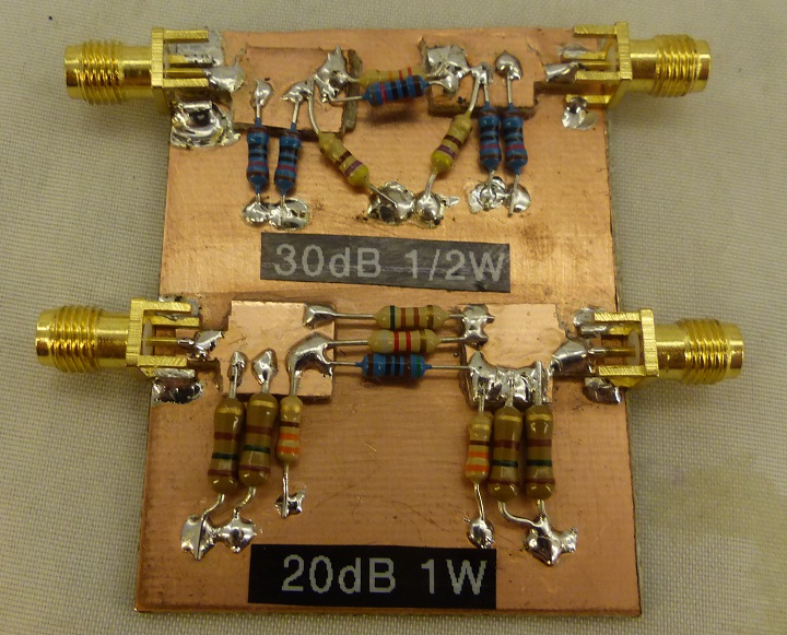
| − | + | == Homebrew RF Attenuators == | |
| − | + | [[file:Atten_30dB_20dV_P1812-720px.jpg]] | |
| − | + | == Attenuators == | |
| − | |||
| − | |||
| − | |||
| − | |||
| − | |||
| − | |||
| − | |||
| − | |||
| − | |||
| − | |||
| − | |||
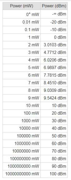
| − | + | [[file:Chart_mW_vs_dbM.PNG]] | |
| − | + | === 30 dB Attenuator === | |
| − | |||
| − | |||
| − | |||
| − | |||
| − | |||
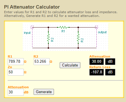
| − | + | * [http://leleivre.com/rf_pipad.html Pi Attenuator Calculator] | |
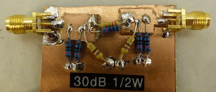
| − | + | [[file:Atten30dB_P116-720px.jpg]] | |
| − | + | [[file:30dB_Attenuator.PNG]] | |
| − | * | + | * Built |
| + | ** Standard 5% resistor values | ||
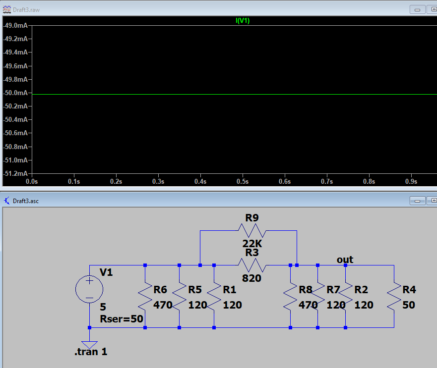
| + | ** R1 = 820 in parallel with 22K = 790.6 ohms | ||
| + | ** R2 = 2 paralleled 120 Ohm 1/4W resistors paralleled with 470 ohms = 53.2 ohms | ||
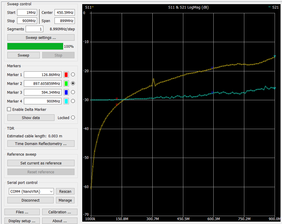
| + | ** Flat from 0-30 MHz | ||
| + | ** Measured attenuation is flat | ||
| + | *** -30.01dB at 1 MHz | ||
| + | *** -30.24dB at 30 MHz | ||
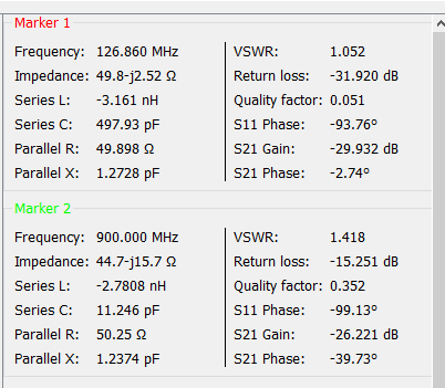
| + | ** Input Impedance - 53.1 ohms, 21.3nF | ||
| + | ** SWR 1.06 | ||
| + | ** 1/2W max (5VDC max, 0 ohm source) | ||
| − | + | * NanoVNA scan data | |
| − | [[ | + | [[file:30dB_Attenuator_NanoVNA_Setup_Curve_900MHz.PNG]] |
| + | |||
| + | [[file:30dB_Attenuator_NanoVNA_Data_900MHz.PNG]] | ||
| + | |||
| + | * LTSPICE Simulation | ||
| + | |||
| + | [[file:LTSPice_30dB.PNG]] | ||
| + | |||
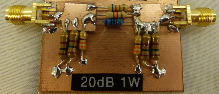
| + | === 20 dB Attenuator === | ||
| + | |||
| + | [[file:Atten_20dB_P115-720px.jpg]] | ||
| + | |||
| + | [[file:20dB_Attenuator.PNG]] | ||
| + | |||
| + | * Build | ||
| + | ** Standard 5% resistor values | ||
| + | ** R1 = 2 of 510 in parallel also in parallel with 8.2K = 247.3 ohms | ||
| + | ** R2 = 2 paralleled 150 Ohm 1/2W resistors paralleled with 330 ohms = 61.11 ohms | ||
| + | ** Flat from 0-30 MHz | ||
| + | ** Measured attenuation is flat | ||
| + | ** Input Impedance - tbd ohms, tbd nF | ||
| + | ** SWR tbd | ||
| + | ** 1W max (8.6 V max, 0 ohm source) | ||
| + | |||
| + | [[file:20dB_Attenuator_NanoVNA_Setup_Curve_900MHz.PNG]] | ||
| + | |||
| + | [[file:20dB_Attenuator_NanoVNA_Data_900MHz.PNG]] | ||
| + | |||
| + | * LTSPICE Simulation | ||
| + | |||
| + | [[file:LTSPice_20dB.PNG]] | ||
| + | |||
| + | === 10 dB Attenuator === | ||
| + | |||
| + | [[file:Atten_10dB_P115-720px.jpg]] | ||
| + | |||
| + | [[file:10dB_Attenuator.PNG]] | ||
| + | |||
| + | * Build | ||
| + | ** Standard 5% resistor values | ||
| + | ** R1 = 2 of 150 in parallel also in parallel with 1.5K = 71.43 ohms (0.3% error) | ||
| + | ** R2 = 3 of 330 Ohm 1/4W parallel resistors paralleled with 810 ohms = 96.85 ohms (0.62% error) | ||
| + | ** Flat from 0-30 MHz | ||
| + | ** Measured attenuation is flat | ||
| + | ** Input Impedance - tbd ohms, tbd nF | ||
| + | ** SWR tbd | ||
| + | ** 3/4W max (9.1 V max, 0 ohm source) | ||
| + | |||
| + | [[file:10dB_Attenuator_NanoVNA_Setup_Curve_900MHz.PNG]] | ||
| + | |||
| + | [[file:10dB_Attenuator_NanoVNA_Data_900MHz.PNG]] | ||
| + | |||
| + | * LTSPICE Simulation | ||
| + | |||
| + | [[file:LTSPice_10dB.PNG]] | ||
| + | |||
| + | === Attenuator Construction === | ||
| + | |||
| + | * Single side copper clad PCB | ||
| + | ** Approx 2"x1" | ||
| + | * Clean with steel wool | ||
| + | * Solder SMA connectors | ||
| + | ** Use large alligator clips to hold while soldering | ||
| + | ** Solder on sides only | ||
| + | |||
| + | [[file:Atten_01_SMAs_720px.jpg]] | ||
| + | |||
| + | * Cut "T" Shaped pads | ||
| + | ** I used nibbler | ||
| + | * Center fits between connector ground pins | ||
| + | * Glue down pads with Superglue | ||
| + | |||
| + | [[file:Atten_02_Pads_720px.jpg]] | ||
| + | |||
| + | * Solder center pin with big solder blob | ||
| + | ** A bit too high for direct contact | ||
| + | * Verify raised pad does not short to ground | ||
| + | |||
| + | [[file:Atten_03_Solder CenterPads_720px.jpg]] | ||
| + | |||
| + | * Solder side resistor(s) | ||
| + | * Leave room for center resistor(s) | ||
| + | |||
| + | [[file:Atten_04_Solder Side_Resistors_720px.jpg]] | ||
| + | |||
| + | * Measure side resistors from pad to ground | ||
| + | * Should match value | ||
| + | * Solder center resistor(s) | ||
| + | |||
| + | [[file:Atten_05_Solder Center_Resistors_720px.jpg]] | ||
| + | |||
| + | * Verify no shorts between centers and ground | ||
| + | |||
| + | == References == | ||
| + | |||
| + | <video type="youtube">A5gGeV7CiQ0</video> | ||
Revision as of 11:50, 7 September 2021
Contents
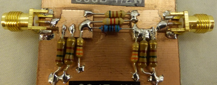
Homebrew RF Attenuators
Attenuators
30 dB Attenuator
- Built
- Standard 5% resistor values
- R1 = 820 in parallel with 22K = 790.6 ohms
- R2 = 2 paralleled 120 Ohm 1/4W resistors paralleled with 470 ohms = 53.2 ohms
- Flat from 0-30 MHz
- Measured attenuation is flat
- -30.01dB at 1 MHz
- -30.24dB at 30 MHz
- Input Impedance - 53.1 ohms, 21.3nF
- SWR 1.06
- 1/2W max (5VDC max, 0 ohm source)
- NanoVNA scan data
- LTSPICE Simulation
20 dB Attenuator
- Build
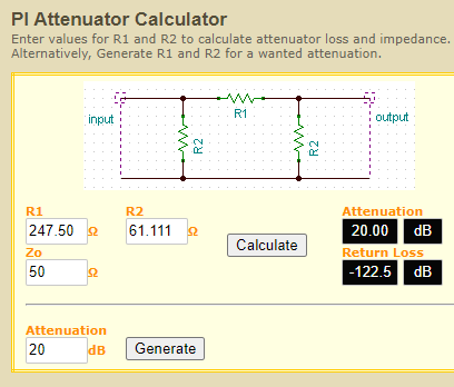
- Standard 5% resistor values
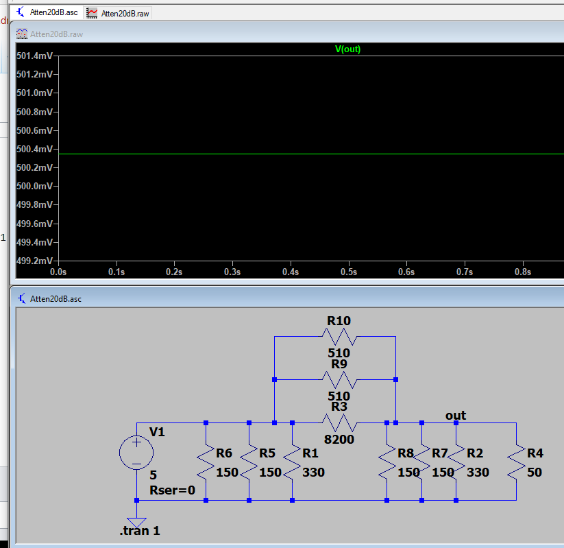
- R1 = 2 of 510 in parallel also in parallel with 8.2K = 247.3 ohms
- R2 = 2 paralleled 150 Ohm 1/2W resistors paralleled with 330 ohms = 61.11 ohms
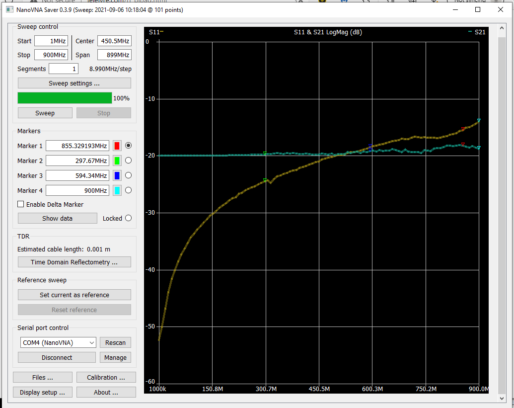
- Flat from 0-30 MHz
- Measured attenuation is flat
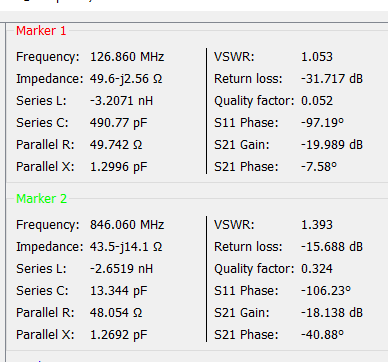
- Input Impedance - tbd ohms, tbd nF
- SWR tbd
- 1W max (8.6 V max, 0 ohm source)
- LTSPICE Simulation
10 dB Attenuator
File:Atten 10dB P115-720px.jpg
- Build
- Standard 5% resistor values
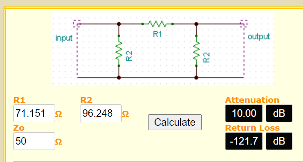
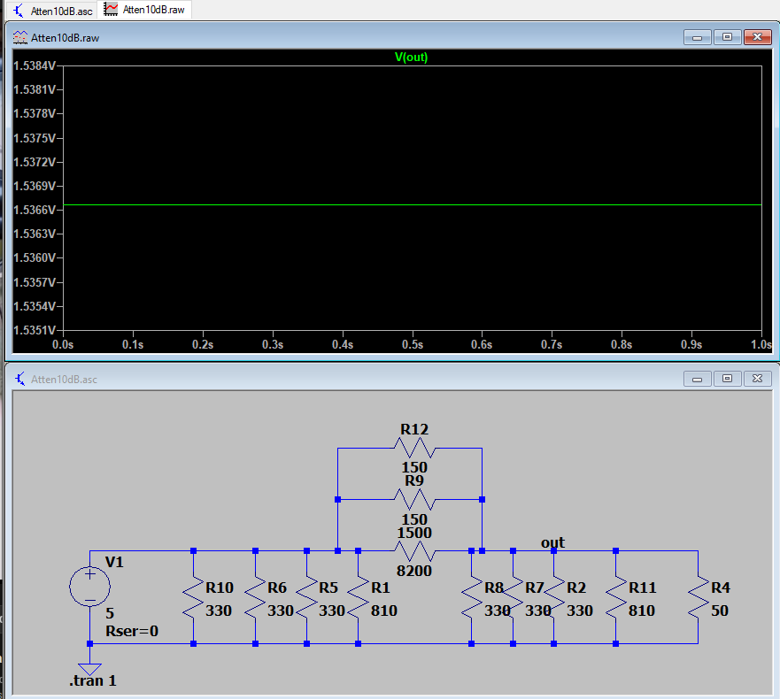
- R1 = 2 of 150 in parallel also in parallel with 1.5K = 71.43 ohms (0.3% error)
- R2 = 3 of 330 Ohm 1/4W parallel resistors paralleled with 810 ohms = 96.85 ohms (0.62% error)
- Flat from 0-30 MHz
- Measured attenuation is flat
- Input Impedance - tbd ohms, tbd nF
- SWR tbd
- 3/4W max (9.1 V max, 0 ohm source)
File:10dB Attenuator NanoVNA Setup Curve 900MHz.PNG
File:10dB Attenuator NanoVNA Data 900MHz.PNG
- LTSPICE Simulation
Attenuator Construction
- Single side copper clad PCB
- Approx 2"x1"
- Clean with steel wool
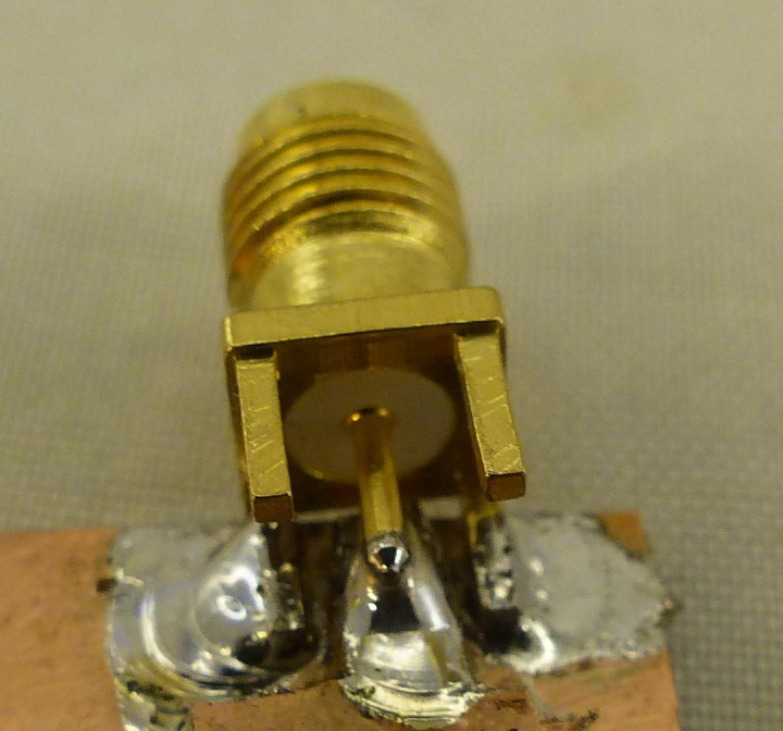
- Solder SMA connectors
- Use large alligator clips to hold while soldering
- Solder on sides only
- Cut "T" Shaped pads
- I used nibbler
- Center fits between connector ground pins
- Glue down pads with Superglue
- Solder center pin with big solder blob
- A bit too high for direct contact
- Verify raised pad does not short to ground
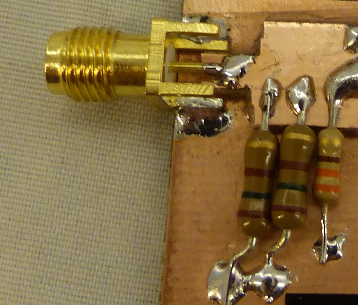
- Solder side resistor(s)
- Leave room for center resistor(s)
- Measure side resistors from pad to ground
- Should match value
- Solder center resistor(s)
- Verify no shorts between centers and ground
References
