Features
- This is an FPGA card in a box with support hardware
- Provides a standardized interface for all FPGA Retrocomputer builds
Retro-Computer Builds
Multicomp Builds
Other Builds
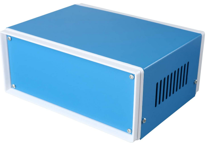
Enclosure

Card Set
QM Tech Cyclone V FPGA Board Features
- QM Tech Cyclone V FPGA Board
- QMTECH Altera Intel FPGA Core Board Cyclone V CycloneV 5CEFA2F23 SDRAM
- QMTECH GitHub page
- On-Board FPGA: 5CEFA2F23I7N
- On-Board FPGA external crystal frequency: 50MHz
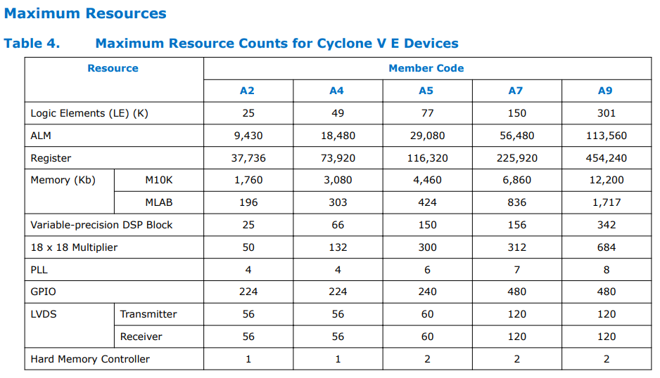
- 5CEFA2F23 has rich RAM resource up to 1,760Kb
- 5CEFA2F23 has 25K logic cells
- On-Board Micron MT25QL128A SPI Flash, 16M bytes for user configuration code
- On-Board Winbond 32MB SDRAM, W9825G6KH-6
- On-Board 3.3V power supply for FPGA by using MP2315 wide input range DC/DC
- 5CEFA2F23 core board has two 64p, 2.54mm pitch headers for extending 108 user IOs. All 108 user IOs are precisely designed with length matching
- 5CEFA2F23 core board has 3 user switches
- 5CEFA2F23 core board has 2 user LEDs
- 5CEFA2F23 core board has JTAG interface, by using 10p, 2.54mm pitch header
- 5CEFA2F23 core board PCB size is: 6.7cm x 8.4cm
- Default power source for board is: 1A@5V DC, the DC header type: DC-050, 5.5mmx2.1mm
Cyclone V_FPGA Resources

- Power LED - D4 (On when 5V is applied)
- User LED - LED_D5 - FPGA Pin_D17 (pull low to illuminate LED)
- KEY0 - SW1 - FPGA Pin_AB13
- RESET_N- SW2 - FPGA PIN_V18
- nCONFIG - SW3 - FPGA PIN_A4
- JP5 - 5V
- Clock - FPGA PIN_M9
Pin List (5CEFA2F23I7)
# -------------------------------------------------------------------------- #
#
# Copyright (C) 2018  Intel Corporation. All rights reserved.
# Your use of Intel Corporation's design tools, logic functions
# and other software and tools, and its AMPP partner logic
# functions, and any output files from any of the foregoing
# (including device programming or simulation files), and any
# associated documentation or information are expressly subject
# to the terms and conditions of the Intel Program License
# Subscription Agreement, the Intel Quartus Prime License Agreement,
# the Intel FPGA IP License Agreement, or other applicable license
# agreement, including, without limitation, that your use is for
# the sole purpose of programming logic devices manufactured by
# Intel and sold by Intel or its authorized distributors.  Please
# refer to the applicable agreement for further details.
#
# -------------------------------------------------------------------------- #
#
# Quartus Prime
# Version 18.1.0 Build 625 09/12/2018 SJ Lite Edition
# Date created = 07:21:26  July 04, 2020
#
# -------------------------------------------------------------------------- #
#
# Notes:
#
# 1) The default values for assignments are stored in the file:
#		TS2_68000_assignment_defaults.qdf
#    If this file doesn't exist, see file:
#		assignment_defaults.qdf
#
# 2) Altera recommends that you do not modify this file. This
#    file is updated automatically by the Quartus Prime software
#    and any changes you make may be lost or overwritten.
#
# -------------------------------------------------------------------------- #

set_global_assignment -name FAMILY "Cyclone V"
set_global_assignment -name DEVICE 5CEFA2F23I7
set_global_assignment -name TOP_LEVEL_ENTITY TS2_68000_Top
set_global_assignment -name ORIGINAL_QUARTUS_VERSION 18.1.0
set_global_assignment -name PROJECT_CREATION_TIME_DATE "07:21:26  JULY 04, 2020"
set_global_assignment -name LAST_QUARTUS_VERSION "21.1.0 Lite Edition"
set_global_assignment -name PROJECT_OUTPUT_DIRECTORY output_files
set_global_assignment -name MIN_CORE_JUNCTION_TEMP "-40"
set_global_assignment -name MAX_CORE_JUNCTION_TEMP 100
set_global_assignment -name ERROR_CHECK_FREQUENCY_DIVISOR 1
set_global_assignment -name EDA_SIMULATION_TOOL "Questa Intel FPGA (VHDL)"
set_global_assignment -name EDA_TIME_SCALE "1 ps" -section_id eda_simulation
set_global_assignment -name EDA_OUTPUT_DATA_FORMAT VHDL -section_id eda_simulation
set_global_assignment -name PARTITION_NETLIST_TYPE SOURCE -section_id Top
set_global_assignment -name PARTITION_FITTER_PRESERVATION_LEVEL PLACEMENT_AND_ROUTING -section_id Top
set_global_assignment -name PARTITION_COLOR 16764057 -section_id Top
set_global_assignment -name POWER_PRESET_COOLING_SOLUTION "23 MM HEAT SINK WITH 200 LFPM AIRFLOW"
set_global_assignment -name POWER_BOARD_THERMAL_MODEL "NONE (CONSERVATIVE)"
set_global_assignment -name TIMING_ANALYZER_MULTICORNER_ANALYSIS ON
set_global_assignment -name SMART_RECOMPILE ON
set_global_assignment -name STRATIX_DEVICE_IO_STANDARD "3.3-V LVTTL"
set_global_assignment -name ENABLE_SIGNALTAP OFF
set_global_assignment -name USE_SIGNALTAP_FILE stp1.stp
set_global_assignment -name ENABLE_OCT_DONE OFF
set_global_assignment -name ENABLE_CONFIGURATION_PINS OFF
set_global_assignment -name ENABLE_BOOT_SEL_PIN OFF
set_global_assignment -name USE_CONFIGURATION_DEVICE OFF
set_global_assignment -name CRC_ERROR_OPEN_DRAIN OFF
set_global_assignment -name RESERVE_FLASH_NCE_AFTER_CONFIGURATION "USE AS REGULAR IO"
set_global_assignment -name OUTPUT_IO_TIMING_NEAR_END_VMEAS "HALF VCCIO" -rise
set_global_assignment -name OUTPUT_IO_TIMING_NEAR_END_VMEAS "HALF VCCIO" -fall
set_global_assignment -name OUTPUT_IO_TIMING_FAR_END_VMEAS "HALF SIGNAL SWING" -rise
set_global_assignment -name OUTPUT_IO_TIMING_FAR_END_VMEAS "HALF SIGNAL SWING" -fall
set_global_assignment -name CYCLONEII_RESERVE_NCEO_AFTER_CONFIGURATION "USE AS REGULAR IO"
set_global_assignment -name RESERVE_DATA1_AFTER_CONFIGURATION "USE AS REGULAR IO"
set_global_assignment -name RESERVE_DATA0_AFTER_CONFIGURATION "USE AS REGULAR IO"
set_global_assignment -name RESERVE_DCLK_AFTER_CONFIGURATION "USE AS REGULAR IO"
set_global_assignment -name NUM_PARALLEL_PROCESSORS ALL
# Clock and reset
set_location_assignment PIN_M9 -to i_CLOCK_50
set_location_assignment PIN_N16 -to i_n_reset
set_instance_assignment -name WEAK_PULL_UP_RESISTOR ON -to i_n_reset
# Serial
set_location_assignment PIN_B11 -to i_cts1
set_instance_assignment -name WEAK_PULL_UP_RESISTOR ON -to i_cts1
set_location_assignment PIN_F10 -to o_rts1
set_location_assignment PIN_C11 -to i_rxd1
set_instance_assignment -name WEAK_PULL_UP_RESISTOR ON -to i_rxd1
set_location_assignment PIN_G10 -to o_txd1
set_location_assignment PIN_L17 -to i_serSelect
set_instance_assignment -name WEAK_PULL_UP_RESISTOR ON -to i_serSelect
# SRAM
set_location_assignment PIN_E2 -to o_n_sRamCS
set_location_assignment PIN_L2 -to o_n_sRamOE
set_location_assignment PIN_D6 -to o_n_sRamWE
set_location_assignment PIN_E9 -to o_sramAddress[19]
set_location_assignment PIN_B5 -to o_sramAddress[18]
set_location_assignment PIN_B6 -to o_sramAddress[17]
set_location_assignment PIN_A7 -to o_sramAddress[16]
set_location_assignment PIN_A10 -to o_sramAddress[15]
set_location_assignment PIN_A8 -to o_sramAddress[14]
set_location_assignment PIN_B7 -to o_sramAddress[13]
set_location_assignment PIN_A5 -to o_sramAddress[12]
set_location_assignment PIN_D9 -to o_sramAddress[11]
set_location_assignment PIN_C6 -to o_sramAddress[10]
set_location_assignment PIN_E7 -to o_sramAddress[9]
set_location_assignment PIN_G2 -to o_sramAddress[8]
set_location_assignment PIN_N2 -to o_sramAddress[7]
set_location_assignment PIN_U2 -to o_sramAddress[6]
set_location_assignment PIN_W2 -to o_sramAddress[5]
set_location_assignment PIN_Y3 -to o_sramAddress[4]
set_location_assignment PIN_U1 -to o_sramAddress[3]
set_location_assignment PIN_N1 -to o_sramAddress[2]
set_location_assignment PIN_L1 -to o_sramAddress[1]
set_location_assignment PIN_G1 -to o_sramAddress[0]
set_location_assignment PIN_C1 -to io_sramData[0]
set_location_assignment PIN_G6 -to io_sramData[1]
set_location_assignment PIN_G8 -to io_sramData[2]
set_location_assignment PIN_F7 -to io_sramData[3]
set_location_assignment PIN_H8 -to io_sramData[4]
set_location_assignment PIN_H6 -to io_sramData[5]
set_location_assignment PIN_C2 -to io_sramData[6]
set_location_assignment PIN_D3 -to io_sramData[7]
# External SD Card
set_location_assignment PIN_M22 -to o_sdCS
set_location_assignment PIN_L18 -to i_sdMISO
set_instance_assignment -name WEAK_PULL_UP_RESISTOR ON -to i_sdMISO
set_location_assignment PIN_L22 -to o_sdMOSI
set_location_assignment PIN_L19 -to o_sdSCLK
set_location_assignment PIN_D17 -to o_driveLED
# Video
set_location_assignment PIN_A15 -to o_hSync
set_location_assignment PIN_A14 -to o_vSync
set_location_assignment PIN_D12 -to o_videoR1
set_location_assignment PIN_E12 -to o_videoR0
set_location_assignment PIN_C13 -to o_videoG1
set_location_assignment PIN_D13 -to o_videoG0
set_location_assignment PIN_A13 -to o_videoB1
set_location_assignment PIN_B13 -to o_videoB0
# PS/2
set_location_assignment PIN_AA2 -to io_ps2Clk
set_instance_assignment -name WEAK_PULL_UP_RESISTOR ON -to io_ps2Clk
set_location_assignment PIN_AA1 -to io_ps2Data
set_instance_assignment -name WEAK_PULL_UP_RESISTOR ON -to io_ps2Data
# 50-pin I/O Connector
set_location_assignment PIN_AB15 -to IO_PIN[3]
set_location_assignment PIN_AA15 -to IO_PIN[4]
set_location_assignment PIN_Y14 -to IO_PIN[5]
set_location_assignment PIN_Y15 -to IO_PIN[6]
set_location_assignment PIN_AB17 -to IO_PIN[7]
set_location_assignment PIN_AB18 -to IO_PIN[8]
set_location_assignment PIN_Y16 -to IO_PIN[9]
set_location_assignment PIN_Y17 -to IO_PIN[10]
set_location_assignment PIN_AA17 -to IO_PIN[11]
set_location_assignment PIN_AA18 -to IO_PIN[12]
set_location_assignment PIN_AA19 -to IO_PIN[13]
set_location_assignment PIN_AA20 -to IO_PIN[14]
set_location_assignment PIN_Y19 -to IO_PIN[15]
set_location_assignment PIN_Y20 -to IO_PIN[16]
set_location_assignment PIN_AB20 -to IO_PIN[17]
set_location_assignment PIN_AB21 -to IO_PIN[18]
set_location_assignment PIN_AB22 -to IO_PIN[19]
set_location_assignment PIN_AA22 -to IO_PIN[20]
set_location_assignment PIN_Y22 -to IO_PIN[21]
set_location_assignment PIN_W22 -to IO_PIN[22]
set_location_assignment PIN_W21 -to IO_PIN[23]
set_location_assignment PIN_Y21 -to IO_PIN[24]
set_location_assignment PIN_V21 -to IO_PIN[25]
set_location_assignment PIN_U22 -to IO_PIN[26]
set_location_assignment PIN_W19 -to IO_PIN[27]
set_location_assignment PIN_V20 -to IO_PIN[28]
set_location_assignment PIN_U20 -to IO_PIN[29]
set_location_assignment PIN_U21 -to IO_PIN[30]
set_location_assignment PIN_T22 -to IO_PIN[31]
set_location_assignment PIN_R22 -to IO_PIN[32]
set_location_assignment PIN_R21 -to IO_PIN[33]
set_location_assignment PIN_P22 -to IO_PIN[34]
set_location_assignment PIN_T19 -to IO_PIN[35]
set_location_assignment PIN_T20 -to IO_PIN[36]
set_location_assignment PIN_P17 -to IO_PIN[37]
set_location_assignment PIN_P16 -to IO_PIN[38]
set_location_assignment PIN_N21 -to IO_PIN[39]
set_location_assignment PIN_N20 -to IO_PIN[40]
set_location_assignment PIN_M20 -to IO_PIN[41]
set_location_assignment PIN_M21 -to IO_PIN[42]
set_location_assignment PIN_N19 -to IO_PIN[43]
set_location_assignment PIN_M18 -to IO_PIN[44]
# SDRAM
set_location_assignment PIN_AA7 -to n_sdRamCas
set_location_assignment PIN_AB5 -to n_sdRamCe
set_location_assignment PIN_AB6 -to n_sdRamRas
set_location_assignment PIN_W9 -to n_sdRamWe
set_location_assignment PIN_P9 -to sdRamAddr[14]
set_location_assignment PIN_T7 -to sdRamAddr[13]
set_location_assignment PIN_Y9 -to sdRamAddr[12]
set_location_assignment PIN_T9 -to sdRamAddr[11]
set_location_assignment PIN_R6 -to sdRamAddr[10]
set_location_assignment PIN_W8 -to sdRamAddr[9]
set_location_assignment PIN_T8 -to sdRamAddr[8]
set_location_assignment PIN_U8 -to sdRamAddr[7]
set_location_assignment PIN_V6 -to sdRamAddr[6]
set_location_assignment PIN_U7 -to sdRamAddr[5]
set_location_assignment PIN_U6 -to sdRamAddr[4]
set_location_assignment PIN_N6 -to sdRamAddr[3]
set_location_assignment PIN_N8 -to sdRamAddr[2]
set_location_assignment PIN_P7 -to sdRamAddr[1]
set_location_assignment PIN_P8 -to sdRamAddr[0]
set_location_assignment PIN_AB11 -to sdRamClk
set_location_assignment PIN_V9 -to sdRamClkEn
set_location_assignment PIN_P12 -to sdRamData[15]
set_location_assignment PIN_R12 -to sdRamData[14]
set_location_assignment PIN_U12 -to sdRamData[13]
set_location_assignment PIN_R11 -to sdRamData[12]
set_location_assignment PIN_R10 -to sdRamData[11]
set_location_assignment PIN_U11 -to sdRamData[10]
set_location_assignment PIN_T10 -to sdRamData[9]
set_location_assignment PIN_U10 -to sdRamData[8]
set_location_assignment PIN_AA8 -to sdRamData[7]
set_location_assignment PIN_AB8 -to sdRamData[6]
set_location_assignment PIN_AA9 -to sdRamData[5]
set_location_assignment PIN_Y10 -to sdRamData[4]
set_location_assignment PIN_AB10 -to sdRamData[3]
set_location_assignment PIN_AA10 -to sdRamData[2]
set_location_assignment PIN_Y11 -to sdRamData[1]
set_location_assignment PIN_AA12 -to sdRamData[0]
#
set_global_assignment -name VHDL_FILE TS2_68000_Top.vhd
set_global_assignment -name VHDL_FILE "../../MultiComp (VHDL Template)/Components/UART/BaudRate6850.vhd"
set_global_assignment -name VHDL_FILE "../../MultiComp (VHDL Template)/Components/SDCARD/Older_SD_Controllers/sd_controller_NealC.vhd"
set_global_assignment -name VHDL_FILE "../../MultiComp (VHDL Template)/Components/COUNTER/n-bit-gray-counter.vhd"
set_global_assignment -name VHDL_FILE "../../MultiComp (VHDL Template)/Components/Debounce/LongDebounce/debounce.vhd"
set_global_assignment -name VHDL_FILE "../../MultiComp (VHDL Template)/Components/TERMINAL/SBCTextDisplayRGB.vhd"
set_global_assignment -name VHDL_FILE "../../MultiComp (VHDL Template)/Components/TERMINAL/SansBoldRomReduced.vhd"
set_global_assignment -name VHDL_FILE "../../MultiComp (VHDL Template)/Components/TERMINAL/SansBoldRom.vhd"
set_global_assignment -name VHDL_FILE "../../MultiComp (VHDL Template)/Components/TERMINAL/DisplayRam2K.vhd"
set_global_assignment -name VHDL_FILE "../../MultiComp (VHDL Template)/Components/TERMINAL/DisplayRam1K.vhd"
set_global_assignment -name VHDL_FILE "../../MultiComp (VHDL Template)/Components/TERMINAL/CGABoldRomReduced.vhd"
set_global_assignment -name VHDL_FILE "../../MultiComp (VHDL Template)/Components/TERMINAL/CGABoldRom.vhd"
set_global_assignment -name VHDL_FILE "../../MultiComp (VHDL Template)/Components/UART/bufferedUART.vhd"
set_global_assignment -name VHDL_FILE "../../MultiComp (VHDL Template)/Components/CPU/M68000/TG68K_2013/TG68KdotC_Kernel.vhd"
set_global_assignment -name VHDL_FILE "../../MultiComp (VHDL Template)/Components/CPU/M68000/TG68K_2013/TG68K_Pack.vhd"
set_global_assignment -name VHDL_FILE "../../MultiComp (VHDL Template)/Components/CPU/M68000/TG68K_2013/TG68K_ALU.vhd"
set_global_assignment -name VHDL_FILE Components/RAM_16Kx16.vhd
set_global_assignment -name VHDL_FILE Components/RAM_4Kx16.vhd
set_global_assignment -name QIP_FILE Components/Monitor_68K_ROM.qip
set_global_assignment -name QIP_FILE Components/RAM_8Kx16.qip
set_global_assignment -name QIP_FILE "../../MultiComp (VHDL Template)/Components/RAM_Internal/RAM_64KX16.qip"
set_global_assignment -name QIP_FILE RAM_32Kx16.qip
set_instance_assignment -name PARTITION_HIERARCHY root_partition -to | -section_id Top
Power
- 5V Power comes from the USB
- 3.3V regulator on the RETRO-EP4CE15 Card
- H2 pins 2-3 shorted on the RETRO-EP4CE15 card
- Set to route 3.3V to the I/O connector
Cabling
SD Card
| J1 PIN
|
SIGNAL
|
COLOR
|
SD PIN
|
FPGA Pin
|
DIR
|
| 2
|
3.3V
|
ORG
|
7
|
VREG 3.3V
|
OUT (PWR)
|
| 45
|
sdSCLK
|
GRY
|
3
|
L19
|
OUT
|
| 46
|
sdMISO
|
BLU
|
2
|
L18
|
IN
|
| 47
|
sdMOSI
|
WHT
|
4
|
L22
|
OUT
|
| 48
|
sdCS
|
VIO
|
5
|
M22
|
OUT
|
| 49
|
GND
|
GRN
|
1
|
GND
|
OUT (PWR)
|
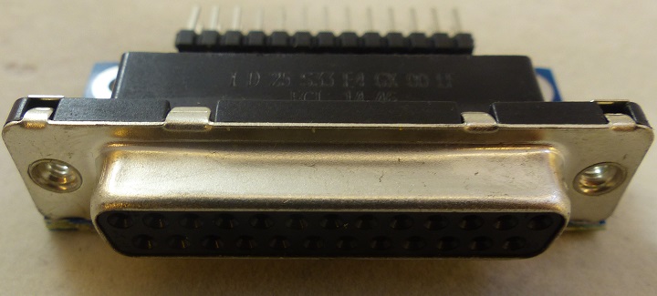
DB-25


USB Panel Mount Connector

Build Photos
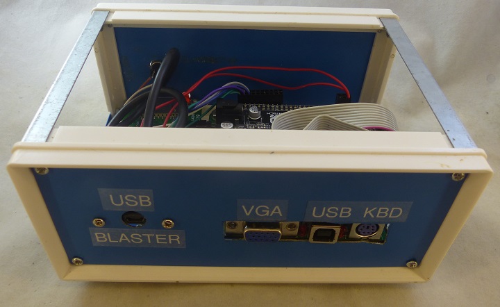
- White-On-Clear P-Touch labels were used to mark front/rear panels
- Rear viewL USB Blaster, VGA, USB-B, PS/2 Keyboard

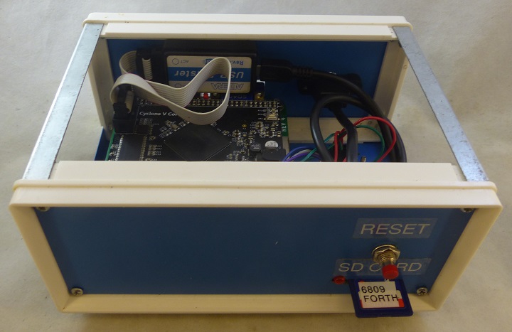
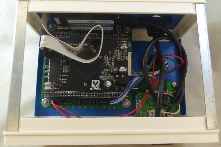
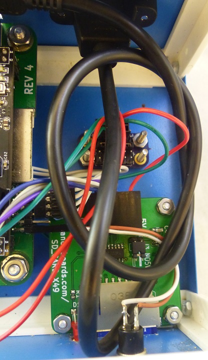
- Top view: FPGA, SD Card, PD01 Power Distribution Card, USB Blaster, internal cabling

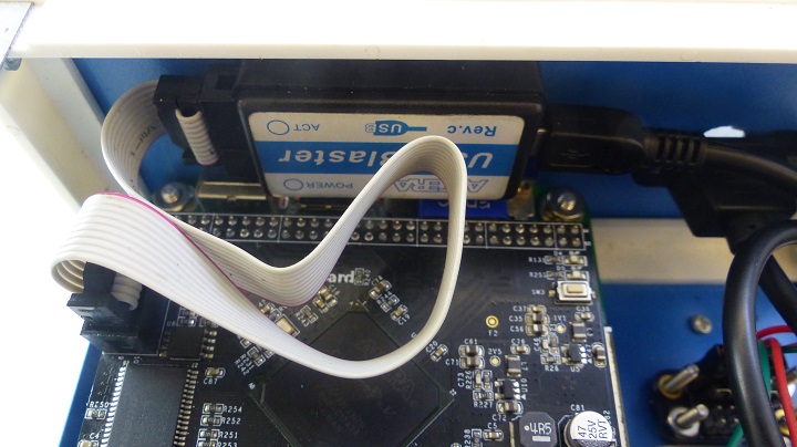
- USB Blaster attached to inside of rear panel using with Double Stick Tape

- Right inside of box: SD Card, Reset switch, PD01 Power Distribution card

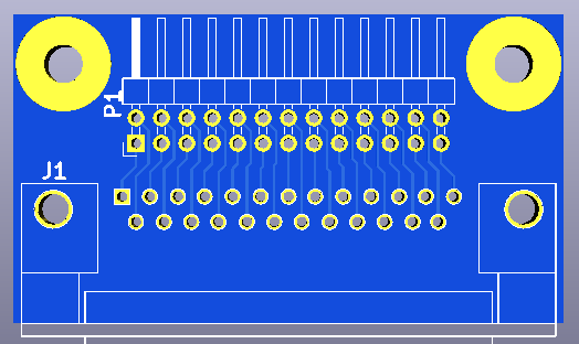
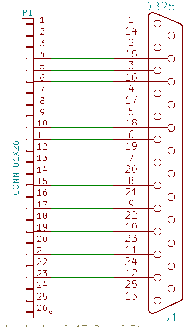
- DB-25 connector card (not shown in enclosure)

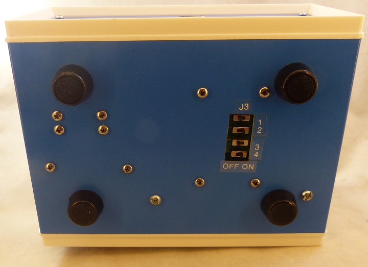
- Selection Switch on the bottom of the bix

GitHub Repository
