Difference between revisions of "VGAX49"
Jump to navigation
Jump to search
Blwikiadmin (talk | contribs) |
Blwikiadmin (talk | contribs) |
||
| (13 intermediate revisions by the same user not shown) | |||
| Line 24: | Line 24: | ||
=== 2:2:2 Resistor Simulation === | === 2:2:2 Resistor Simulation === | ||
| − | * 3.3V Drive | + | * 3.3V Drive out of FPGA |
| + | * 1V is drive level for VGA specification | ||
| + | * 8 mA max drive current | ||
| + | * VGA presents a 75 Ohm load | ||
| + | * Series resistors present a voltage divider between the resistors on the card and the VGA load | ||
| + | * 1V at 75 Ohms is 13.3 mA | ||
| + | * Each color is independently driven | ||
| + | * The resistor with the smallest resistance value has larger current from the FPGA pin | ||
| + | * Current switches from source to sink depending on the voltages on the other resistors | ||
| + | * Use common value, 1% resistors | ||
| + | * 330 Ohm series resistor into a 75 Ohm load is 8.15 mA | ||
| + | ** Voltage with 330/75 ohm voltage divider is 0.61V - not full brightness | ||
| + | * Each resistor is 2X the value of the previous resistor | ||
| + | * Next standard value from 330 ohms is 680 ohms | ||
| + | ** Voltage is 0.83V - better brightness | ||
| + | |||
| + | [[File:VGA_Sim_2R_Current.PNG]] | ||
| + | |||
| + | [[File:VGA_Sim_2R_Voltage.PNG]] | ||
=== 5:6:5 Resistor Simulation === | === 5:6:5 Resistor Simulation === | ||
| − | * 3.3V Drive | + | * 3.3V Drive out of FPGA |
| + | * 1V is drive level for VGA specification | ||
| + | * 8 mA max drive current | ||
| + | * VGA presents a 75 Ohm load | ||
| + | * Series resistors present a voltage divider between the resistors on the card and the VGA load | ||
| + | * 1V at 75 Ohms is 13.3 mA | ||
| + | * Each color is independently driven | ||
| + | * The resistor with the smallest resistance value has larger current from the FPGA pin | ||
| + | * Current switches from source to sink depending on the voltages on the other resistors | ||
| + | * Use common value, 1% resistors | ||
| + | * 330 Ohm series resistor into a 75 Ohm load is 8.15 mA | ||
| + | ** Voltage with 330/75 ohm voltage divider is 0.61V - not full brightness | ||
== Schematic == | == Schematic == | ||
Revision as of 18:08, 13 February 2020
Contents
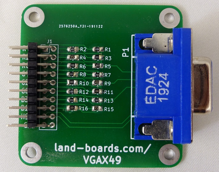
Features
- Digital VGA adapter
- 16-bit digital video
- 5:6:5 (R:G:B) mapping (maximum)
- 2:2:2 (R:G:B) mapping (option)
- Uses summing resistors
- DB-15F connector
- 49x49mm ODAS form factor
- Mounting holes
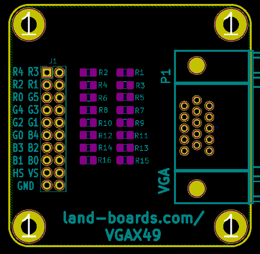
Connectors
J1 - Digital Connections
P1 - VGA connector
Simulation
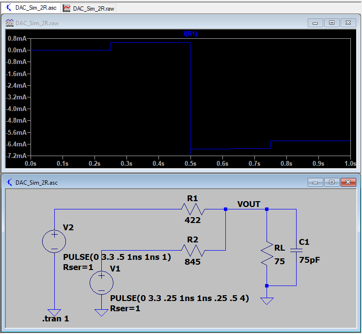
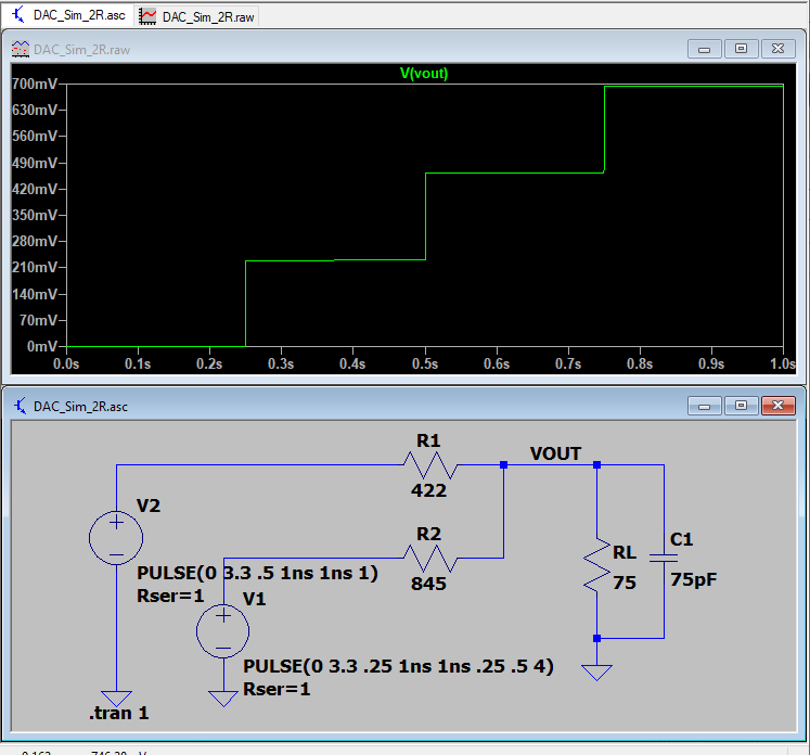
2:2:2 Resistor Simulation
- 3.3V Drive out of FPGA
- 1V is drive level for VGA specification
- 8 mA max drive current
- VGA presents a 75 Ohm load
- Series resistors present a voltage divider between the resistors on the card and the VGA load
- 1V at 75 Ohms is 13.3 mA
- Each color is independently driven
- The resistor with the smallest resistance value has larger current from the FPGA pin
- Current switches from source to sink depending on the voltages on the other resistors
- Use common value, 1% resistors
- 330 Ohm series resistor into a 75 Ohm load is 8.15 mA
- Voltage with 330/75 ohm voltage divider is 0.61V - not full brightness
- Each resistor is 2X the value of the previous resistor
- Next standard value from 330 ohms is 680 ohms
- Voltage is 0.83V - better brightness
5:6:5 Resistor Simulation
- 3.3V Drive out of FPGA
- 1V is drive level for VGA specification
- 8 mA max drive current
- VGA presents a 75 Ohm load
- Series resistors present a voltage divider between the resistors on the card and the VGA load
- 1V at 75 Ohms is 13.3 mA
- Each color is independently driven
- The resistor with the smallest resistance value has larger current from the FPGA pin
- Current switches from source to sink depending on the voltages on the other resistors
- Use common value, 1% resistors
- 330 Ohm series resistor into a 75 Ohm load is 8.15 mA
- Voltage with 330/75 ohm voltage divider is 0.61V - not full brightness


