Difference between pages "File:Dimensions 80x50x20.jpg" and "A Termination Insensitive Amplifier for Bidirectional Transceivers"
(Difference between pages)
Jump to navigation
Jump to search
Blwikiadmin (talk | contribs) |
Blwikiadmin (talk | contribs) |
||
| Line 1: | Line 1: | ||
| + | == A Termination Insensitive Amplifier for Bidirectional Transceivers == | ||
| + | === Through Hole Version === | ||
| + | |||
| + | [[file:TIA_P1015_720px.jpg]] | ||
| + | |||
| + | === Surface Mount Version === | ||
| + | |||
| + | [[file:W7Z01_TIA_SMT_P1837-720PX.jpg]] | ||
| + | |||
| + | == W7ZOI Design == | ||
| + | |||
| + | * Paper - [http://w7zoi.net/bidirectional_matched_amplifier.pdf A Termination Insensitive Amplifier for Bidirectional Transceivers] - W7ZOI (Wes Hayward) design | ||
| + | * [http://w7zoi.net/transistor_models_and_the_fba.pdf Transistor Models and the Feedback Amplifier] | ||
| + | * Termination Insensitive - input impedance that does not depend upon the output load | ||
| + | * Bi-directional - amplifiers in both directions | ||
| + | * 50 ohms in/out | ||
| + | * BNC or SMA Connectors | ||
| + | * Transformer-less | ||
| + | * Power applied to one half at a time - determines signal flow direction | ||
| + | * ~30 mA per side | ||
| + | * SMT or Through Hole versions | ||
| + | ** SMT version fits in 80x50x20mm aluminum case | ||
| + | |||
| + | === W7ZOI Schematic === | ||
| + | |||
| + | [[FILE:W7ZOI_SCHEMATIC.PNG]] | ||
| + | |||
| + | === * Use === | ||
| + | |||
| + | * Between RF/LO mixer (IF output/input) and crystal filter | ||
| + | * Between Crystal Filter and Product Detector / Balanced Modulator | ||
| + | |||
| + | [[file:FARHADPNG.PNG]] | ||
| + | |||
| + | == Schematic in KiCAD == | ||
| + | |||
| + | * [http://land-boards.com/W7ZOI_TIA/W7ZOI_TIA_SCHEMATIC_REV1.pdf Schematic] (pdf file) | ||
| + | * Single channel | ||
| + | * With SPICE directives | ||
| + | |||
| + | [[file:W7ZOI_SCHEMATIC_KiCAD.PNG]] | ||
| + | |||
| + | * Both channels | ||
| + | * With SPICE directives | ||
| + | |||
| + | [[file:W7ZOI_SCHEMATIC_KiCAD-2.PNG]] | ||
| + | |||
| + | == NGSPICE Simulation == | ||
| + | |||
| + | * NGSPICE run from KiCAD | ||
| + | ** [http://ngspice.sourceforge.net/ngspice-eeschema.html Tutorial: ngspice simulation in KiCad/Eeschema] | ||
| + | * +24 dB @12V | ||
| + | * 2N3904 Alternate Node Sequence (MMBT3903 - SOT23) | ||
| + | ** KiCAD order 1 2 3 is the SPICE normal order | ||
| + | ** NGSPICE order: 3 1 2 | ||
| + | |||
| + | [[file:W7ZOI_Simulation_KiCAD-3.PNG]] | ||
| + | |||
| + | * Closely matches | ||
| + | |||
| + | [[file:W7ZOI_Gainz.PNG]] | ||
| + | |||
| + | * Across Band | ||
| + | [[file:W7ZOI_Simulation_KiCAD_S2.PNG]] | ||
| + | |||
| + | == Measurements == | ||
| + | |||
| + | * Powering only L-R side | ||
| + | * 30 mA power supply current | ||
| + | * 12V | ||
| + | |||
| + | === NanoVNA Measurements (Through-hole) === | ||
| + | |||
| + | ==== Left-to-right flow ==== | ||
| + | |||
| + | * At 9 MHz | ||
| + | |||
| + | [[file:L-R_1-30MHz_meas.png]] | ||
| + | |||
| + | * S21 - sweep 1-30 MHz | ||
| + | |||
| + | [[file:L-R_1-30MHz_S21.png]] | ||
| + | |||
| + | * S11 VSWR - sweep 1-30 MHz | ||
| + | |||
| + | [[file:L-R_1-30MHz_S11.png]] | ||
| + | |||
| + | ==== Right-to-Left flow ==== | ||
| + | |||
| + | * At 9 MHz | ||
| + | |||
| + | [[file:R-L_1-30MHz_meas.png]] | ||
| + | |||
| + | * S21 - sweep 1-30 MHz | ||
| + | |||
| + | [[file:R-L__1-30MHz_S21.png]] | ||
| + | |||
| + | * S11 VSWR - sweep 1-30 MHz | ||
| + | |||
| + | [[file:R-L_1-30MHz_S11.png]] | ||
| + | |||
| + | === NanoVNA Measurements (SMT) === | ||
| + | |||
| + | * Re = 150 | ||
| + | ** A bit more gain | ||
| + | |||
| + | ==== Left-to-right flow ==== | ||
| + | |||
| + | * At 9 MHz | ||
| + | |||
| + | [[file:L-R_1-30MHz_meas_SMT.png]] | ||
| + | |||
| + | * S21 - sweep 1-30 MHz | ||
| + | |||
| + | [[file:L-R_1-30MHz_S21_SMT.png]] | ||
| + | |||
| + | * S11 VSWR - sweep 1-30 MHz | ||
| + | |||
| + | [[file:L-R_1-30MHz_S11_SMT.png]] | ||
| + | |||
| + | ==== Right-to-Left flow ==== | ||
| + | |||
| + | * At 9 MHz | ||
| + | |||
| + | [[file:R-L_1-30MHz_meas_SMT.png]] | ||
| + | |||
| + | * S21 - sweep 1-30 MHz | ||
| + | |||
| + | [[file:R-L__1-30MHz_S21_SMT.png]] | ||
| + | |||
| + | * S11 VSWR - sweep 1-30 MHz | ||
| + | |||
| + | [[file:R-L_1-30MHz_S11_SMT.png]] | ||
| + | |||
| + | == CAD == | ||
| + | |||
| + | === Through Hole CAD === | ||
| + | |||
| + | * 2.4" x 2.4" | ||
| + | * 2.0 hole center-to-center | ||
| + | |||
| + | [[FILE:W7ZOI_CAD.PNG]] | ||
| + | |||
| + | === SMT CAD === | ||
| + | |||
| + | [[FILE:W7ZOI_TIA_SMT_CAD.PNG]] | ||
| + | |||
| + | == Test Procedure == | ||
| + | |||
| + | === Test Equipment === | ||
| + | |||
| + | * Unit Under Test (UUT) | ||
| + | * [[NanoVNA]] | ||
| + | * [[RF_Attenuators#Triple_Attenuator|30 dB attenuator]] tap on Triple attenuator | ||
| + | * [[NanoVNA#RF_Demo_Kit|RF Demo Kit]] | ||
| + | * (3) SMA to SMA Male:Male cables | ||
| + | * [[Benchtop Power Supply DPS3005]] | ||
| + | ** 12V Power Supply | ||
| + | ** Current Limit set at 100 mA | ||
| + | |||
| + | === Calibrate NanoVNA === | ||
| + | |||
| + | * Cable #1 from RF out of NanoVNA (upper jack) to left side of 30 dB attenuator | ||
| + | * Cable #2 from right side of 30 dB attenuator to left side of RF Demo Kit | ||
| + | ** Multiple positions for open, through, and short | ||
| + | * Cable #3 from right side of RF Demo Kit to input of NanoVNA (lower jack) | ||
| + | |||
| + | === Test UUT === | ||
| + | |||
| + | * Replace RF Demo Kit with UUT | ||
| + | * Test each direction at a time | ||
| + | ** Power up Left to right, test | ||
| + | ** Power up right to left, test | ||
| + | * Should show gain of about 20 dB at 10 MHz | ||
| + | |||
| + | == Enclosure == | ||
| + | |||
| + | * The SMT version is designed to fit in a [https://www.ebay.com/sch/i.html?_from=R40&_trksid=p2047675.m570.l1313&_nkw=80x50x20mm&_sacat=0 80x50x20mm Extruded Aluminum Project Box] | ||
| + | * [http://land-boards.com/W7ZOI_TIA/W7ZOI_TIA_SMD_CUTOUTS.pdf W7ZOI_TIA_SMD_CUTOUTS.pdf Panel marking template] | ||
| + | |||
| + | [[file:Dimensions_80x50x20.jpg]] | ||
| + | |||
| + | == Videos == | ||
| + | |||
| + | <video type="youtube">JjcxEYk9atg</video> | ||
| + | |||
| + | <video type="youtube">CpQK0W7TY5g</video> | ||
| + | |||
| + | <video type="youtube">7TtKE39TWpI</video> | ||
| + | |||
| + | <video type="youtube">T8lq8Qtjqe0</video> | ||
| + | |||
| + | == Assembly Sheet == | ||
| + | |||
| + | * [[W7ZOI TIA Assembly Sheet - Rev 1]] - Through-hole version | ||
| + | * [[W7ZOI TIA SMT Assembly Sheet - Rev 1]] - SMT version | ||
Latest revision as of 12:13, 26 March 2022
Contents
A Termination Insensitive Amplifier for Bidirectional Transceivers
Through Hole Version

Surface Mount Version

W7ZOI Design
- Paper - A Termination Insensitive Amplifier for Bidirectional Transceivers - W7ZOI (Wes Hayward) design
- Transistor Models and the Feedback Amplifier
- Termination Insensitive - input impedance that does not depend upon the output load
- Bi-directional - amplifiers in both directions
- 50 ohms in/out
- BNC or SMA Connectors
- Transformer-less
- Power applied to one half at a time - determines signal flow direction
- ~30 mA per side
- SMT or Through Hole versions
- SMT version fits in 80x50x20mm aluminum case
W7ZOI Schematic

* Use
- Between RF/LO mixer (IF output/input) and crystal filter
- Between Crystal Filter and Product Detector / Balanced Modulator

Schematic in KiCAD
- Schematic (pdf file)
- Single channel
- With SPICE directives

- Both channels
- With SPICE directives

NGSPICE Simulation
- NGSPICE run from KiCAD
- +24 dB @12V
- 2N3904 Alternate Node Sequence (MMBT3903 - SOT23)
- KiCAD order 1 2 3 is the SPICE normal order
- NGSPICE order: 3 1 2

- Closely matches

- Across Band

Measurements
- Powering only L-R side
- 30 mA power supply current
- 12V
NanoVNA Measurements (Through-hole)
Left-to-right flow
- At 9 MHz

- S21 - sweep 1-30 MHz

- S11 VSWR - sweep 1-30 MHz

Right-to-Left flow
- At 9 MHz

- S21 - sweep 1-30 MHz

- S11 VSWR - sweep 1-30 MHz

NanoVNA Measurements (SMT)
- Re = 150
- A bit more gain
Left-to-right flow
- At 9 MHz

- S21 - sweep 1-30 MHz

- S11 VSWR - sweep 1-30 MHz

Right-to-Left flow
- At 9 MHz

- S21 - sweep 1-30 MHz

- S11 VSWR - sweep 1-30 MHz

CAD
Through Hole CAD
- 2.4" x 2.4"
- 2.0 hole center-to-center

SMT CAD

Test Procedure
Test Equipment
- Unit Under Test (UUT)
- NanoVNA
- 30 dB attenuator tap on Triple attenuator
- RF Demo Kit
- (3) SMA to SMA Male:Male cables
- Benchtop Power Supply DPS3005
- 12V Power Supply
- Current Limit set at 100 mA
Calibrate NanoVNA
- Cable #1 from RF out of NanoVNA (upper jack) to left side of 30 dB attenuator
- Cable #2 from right side of 30 dB attenuator to left side of RF Demo Kit
- Multiple positions for open, through, and short
- Cable #3 from right side of RF Demo Kit to input of NanoVNA (lower jack)
Test UUT
- Replace RF Demo Kit with UUT
- Test each direction at a time
- Power up Left to right, test
- Power up right to left, test
- Should show gain of about 20 dB at 10 MHz
Enclosure
- The SMT version is designed to fit in a 80x50x20mm Extruded Aluminum Project Box
- W7ZOI_TIA_SMD_CUTOUTS.pdf Panel marking template

Videos
Assembly Sheet
- W7ZOI TIA Assembly Sheet - Rev 1 - Through-hole version
- W7ZOI TIA SMT Assembly Sheet - Rev 1 - SMT version
File history
Click on a date/time to view the file as it appeared at that time.
| Date/Time | Thumbnail | Dimensions | User | Comment | |
|---|---|---|---|---|---|
| current | 11:33, 26 March 2022 | 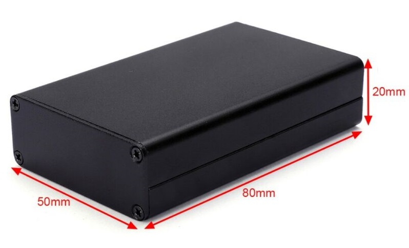 | 798 × 485 (51 KB) | Blwikiadmin (talk | contribs) |
You cannot overwrite this file.
File usage
The following page uses this file: