Difference between revisions of "PDP-8 Front Panel"
Jump to navigation
Jump to search
Blwikiadmin (talk | contribs) (Created page with "File:PDP-8_FRONT.png") |
Blwikiadmin (talk | contribs) |
||
| (37 intermediate revisions by the same user not shown) | |||
| Line 1: | Line 1: | ||
[[File:PDP-8_FRONT.png]] | [[File:PDP-8_FRONT.png]] | ||
| + | |||
| + | == Features == | ||
| + | |||
| + | * 50 pin connector | ||
| + | ** 2x25 Pinout matches [[RETRO-EP4CE15]] Card pins | ||
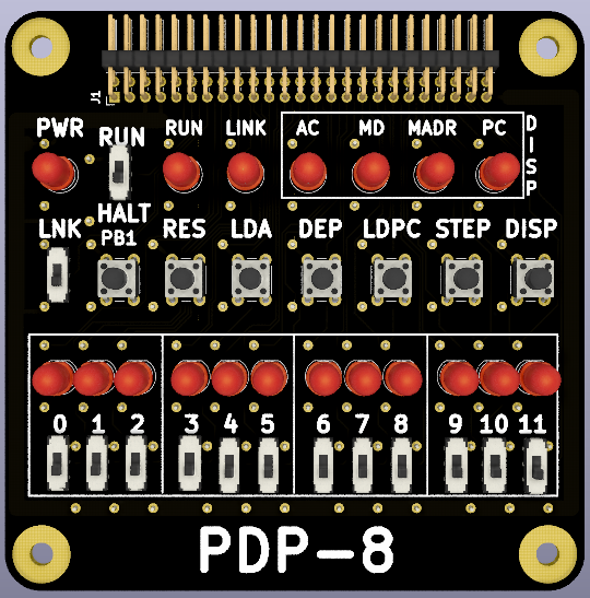
| + | * 12 Value LEDs (DB0-11) - octal format | ||
| + | ** Display options: Program Counter (PC), Memory Address, Memory Data, Accumulator | ||
| + | * 12 Load Value Slide Switches (SL0-11) - octal format | ||
| + | ** Enter values: PC, Memory Address, Memory Data, Accumulator | ||
| + | * LNK - Link value slide switch | ||
| + | * DISP - Display 12 Value LEDs select pushbutton | ||
| + | ** Cycles between LEDs displaying PC, Memory Address, Memory Data, Accumulator | ||
| + | * Pushbutton Switches | ||
| + | ** STEP pushbutton - Increment PC | ||
| + | ** LDPC pushbutton - Load PC from Value Slide Switches | ||
| + | ** DEP pushbutton - Store value from Value Slide Switches to memory | ||
| + | ** LDA pushbutton - Store value from Value Slide Switches to Accumulator | ||
| + | ** RES - Reset pushbutton - Resets CPU | ||
| + | ** PB1 - spare pushbutton | ||
| + | * 4 DISP LEDs - Cycle between 12 LEDs source with DISP pushbutton | ||
| + | ** PC - 12 LEDs display Program Counter value | ||
| + | ** MADR - 12 LEDs display Memory Address value | ||
| + | ** MD - 12 LEDs display Memory Data value | ||
| + | ** AC - 12 LEDs display Accumulator value | ||
| + | * LINK LED - Displays Link value | ||
| + | * RUN LED - Running program | ||
| + | * RUN/HALT slide switch | ||
| + | * PWR - Power LED | ||
| + | * 95x95mm form factor | ||
| + | * (4) 6-32 mounting holes | ||
| + | |||
| + | == PDP-8 FPGA Design == | ||
| + | |||
| + | * [https://www.amazon.com/PDP-8-Class-Project-Resoling-Machine-ebook/dp/B07KY5RCJ7/ The PDP-8 Class Project -or- Resoling an Old Machine by Tom Almy] - Amazon link (Kindle e-boot or paper) | ||
| + | * [https://github.com/douggilliland/Retro-Computers/tree/master/PDP-8/PDP8_Book(Almy) PDP-8 PFGA Design] - GitHub repo | ||
| + | |||
| + | == J1 Connector == | ||
| + | |||
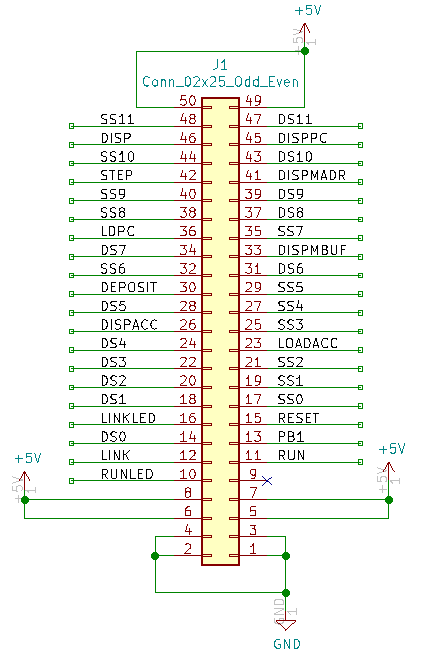
| + | * Extra power and ground pins (not on [[RETRO-EP4CE15]] Card) | ||
| + | ** Pins 3,4 = GND | ||
| + | ** Pins 5-8 = VCC | ||
| + | ** Pin 9 = N/C | ||
| + | |||
| + | [[File:PDP-8F_FrontPanel_Conn.PNG]] | ||
| + | |||
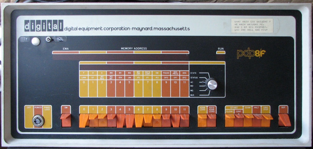
| + | == Real PDP-8/F Front Panel == | ||
| + | |||
| + | [[File:PDP-8F_FrontPanel_720px.jpg]] | ||
| + | |||
| + | == PDP-8 Front Panel Assembly Sheet == | ||
| + | |||
| + | [[PDP-8 Front Panel Assembly Sheet]] | ||
Revision as of 18:40, 24 April 2021
Contents
Features
- 50 pin connector
- 2x25 Pinout matches RETRO-EP4CE15 Card pins
- 12 Value LEDs (DB0-11) - octal format
- Display options: Program Counter (PC), Memory Address, Memory Data, Accumulator
- 12 Load Value Slide Switches (SL0-11) - octal format
- Enter values: PC, Memory Address, Memory Data, Accumulator
- LNK - Link value slide switch
- DISP - Display 12 Value LEDs select pushbutton
- Cycles between LEDs displaying PC, Memory Address, Memory Data, Accumulator
- Pushbutton Switches
- STEP pushbutton - Increment PC
- LDPC pushbutton - Load PC from Value Slide Switches
- DEP pushbutton - Store value from Value Slide Switches to memory
- LDA pushbutton - Store value from Value Slide Switches to Accumulator
- RES - Reset pushbutton - Resets CPU
- PB1 - spare pushbutton
- 4 DISP LEDs - Cycle between 12 LEDs source with DISP pushbutton
- PC - 12 LEDs display Program Counter value
- MADR - 12 LEDs display Memory Address value
- MD - 12 LEDs display Memory Data value
- AC - 12 LEDs display Accumulator value
- LINK LED - Displays Link value
- RUN LED - Running program
- RUN/HALT slide switch
- PWR - Power LED
- 95x95mm form factor
- (4) 6-32 mounting holes
PDP-8 FPGA Design
- The PDP-8 Class Project -or- Resoling an Old Machine by Tom Almy - Amazon link (Kindle e-boot or paper)
- PDP-8 PFGA Design - GitHub repo
J1 Connector
- Extra power and ground pins (not on RETRO-EP4CE15 Card)
- Pins 3,4 = GND
- Pins 5-8 = VCC
- Pin 9 = N/C


