Difference between revisions of "SCF-2"
Jump to navigation
Jump to search
Blwikiadmin (talk | contribs) |
Blwikiadmin (talk | contribs) |
||
| (9 intermediate revisions by the same user not shown) | |||
| Line 10: | Line 10: | ||
* Ring pin brought to connector | * Ring pin brought to connector | ||
** Ring pin is not used in Synth applications | ** Ring pin is not used in Synth applications | ||
| − | ** Card can be used as a 3.5mm breakout | + | ** Card can be used as a 3.5mm breakout (1x5 vertical header mounted to rear) |
* (2) 4-40 mounting holes | * (2) 4-40 mounting holes | ||
| + | * 36mmx28mm | ||
=== Schematic === | === Schematic === | ||
| Line 42: | Line 43: | ||
* 2x4 Header, 0.1" | * 2x4 Header, 0.1" | ||
| + | * Either 2x4 (Stereo) or 1x4 (mono) | ||
| + | ** Install 1x4 on 1,3,5,7 pointing down for breadboard | ||
[[FILE:SCF-2_J3.PNG]] | [[FILE:SCF-2_J3.PNG]] | ||
| Line 55: | Line 58: | ||
# GND | # GND | ||
# GND | # GND | ||
| + | |||
| + | == Build Options == | ||
| + | |||
| + | [[FILE:SCF-2_REV1_CAD.PNG]] | ||
| + | |||
| + | * D1-D3 = Clamping diodes | ||
| + | * R1, R2 = Series resistor | ||
| + | * R3, R4 - scaling resistors | ||
| + | * C1, C2 - Parallel capacitor | ||
| + | * J3, 1x4 or 2x4 (above) | ||
| + | |||
| + | === Build as Adapter (No SCF) === | ||
| + | |||
| + | * Just install 0 Ohms series resistor at R1, R2 | ||
| + | |||
| + | === Build as Buffered Connection=== | ||
| + | |||
| + | * Install series resistors at R1, R2 | ||
| + | |||
| + | === Build as Filter Without Clamping === | ||
| + | |||
| + | * R1/C1 filter | ||
| + | * R2/C2 filter | ||
| + | |||
| + | == Mechanicals == | ||
| + | |||
| + | [[FILE:SCF-2_REV1_MECHS.PNG]] | ||
Latest revision as of 21:47, 4 October 2022
Contents
Features
- Digital Inputs or Outputs
- (2) 3.5mm Jacks
- Scaling resistors
- Schottky Clamping Diodes
- Filter cap
- Ring pin brought to connector
- Ring pin is not used in Synth applications
- Card can be used as a 3.5mm breakout (1x5 vertical header mounted to rear)
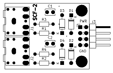
- (2) 4-40 mounting holes
- 36mmx28mm
Schematic
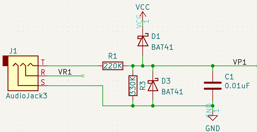
Used as Digital Input
- 550K input impedance presents light load
- R1/R3 - Input scale resistors
- Ex: 5.0V control voltage to 3.0 V
- Clipping diodes protect inputs
- R1/C1 create input filter = 2.2mS = 454 Hz
Used as Digital Output
- Drive with 5V low output impedance source
- DNP R3, C1
- Use lower value for R1 (typically 200 Ohms, etc)
- Can leave Clipping Diodes to protect driver
Connectors
J1, J2 - 3.5mm Jacks
- Tip
- Sleeve
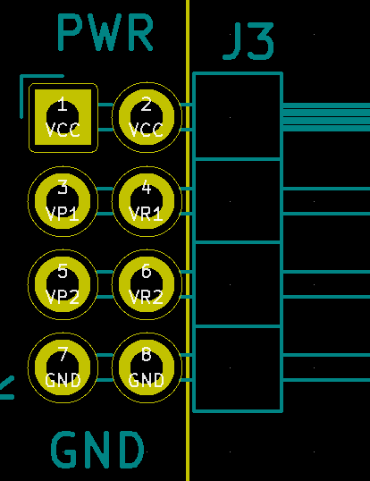
J3 - I/O Connector
- 2x4 Header, 0.1"
- Either 2x4 (Stereo) or 1x4 (mono)
- Install 1x4 on 1,3,5,7 pointing down for breadboard
- Pinout
- VCC
- VCC
- VP1 - Tip J1
- VR1 - Ring J1 (not used in Synth applications)
- VP2 - Tip J2
- VR2 - Ring J2 (not used in Synth applications)
- GND
- GND
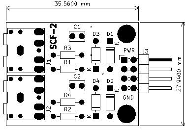
Build Options
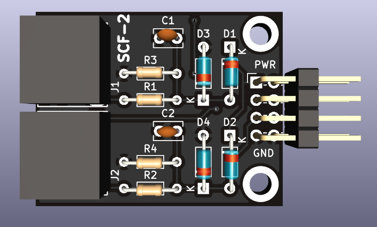
- D1-D3 = Clamping diodes
- R1, R2 = Series resistor
- R3, R4 - scaling resistors
- C1, C2 - Parallel capacitor
- J3, 1x4 or 2x4 (above)
Build as Adapter (No SCF)
- Just install 0 Ohms series resistor at R1, R2
Build as Buffered Connection
- Install series resistors at R1, R2
Build as Filter Without Clamping
- R1/C1 filter
- R2/C2 filter
