Difference between revisions of "LB-65CXX-01"
Jump to navigation
Jump to search
Blwikiadmin (talk | contribs) |
Blwikiadmin (talk | contribs) |
||
| Line 1: | Line 1: | ||
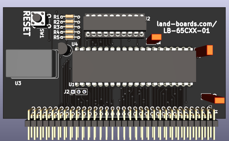
[[file:LB-65C816-01_FRONT_REV1(BLK).png]] | [[file:LB-65C816-01_FRONT_REV1(BLK).png]] | ||
| − | == Features | + | == Features == |
* 65C02 or 65C816 CPU | * 65C02 or 65C816 CPU | ||
Revision as of 19:20, 18 August 2024
Features
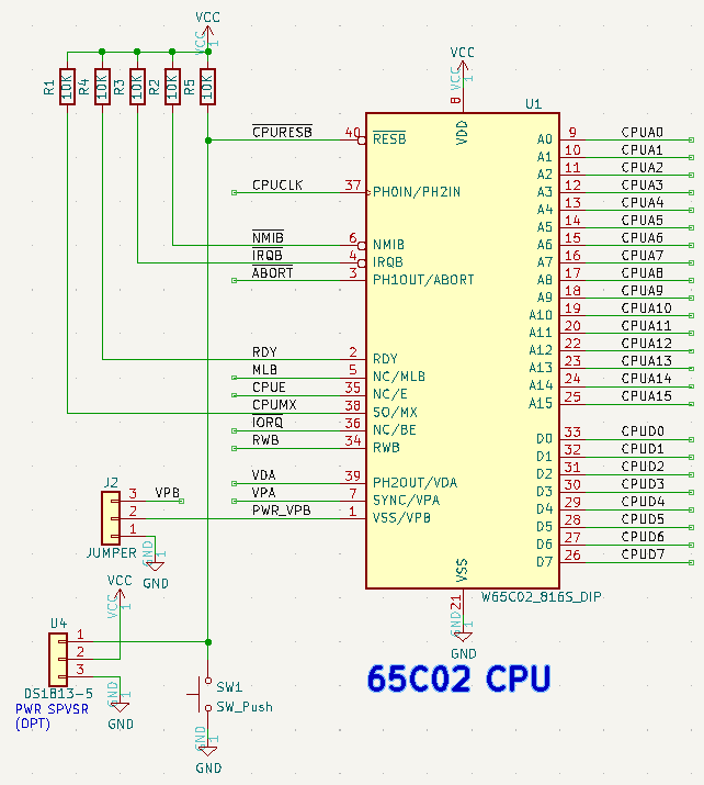
- 65C02 or 65C816 CPU
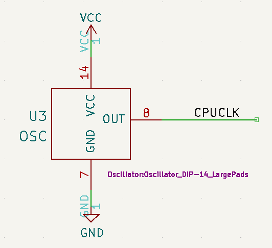
- 2 MHz Oscillator on card
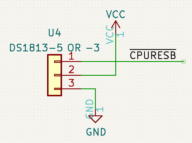
- Reset switch/power monitor
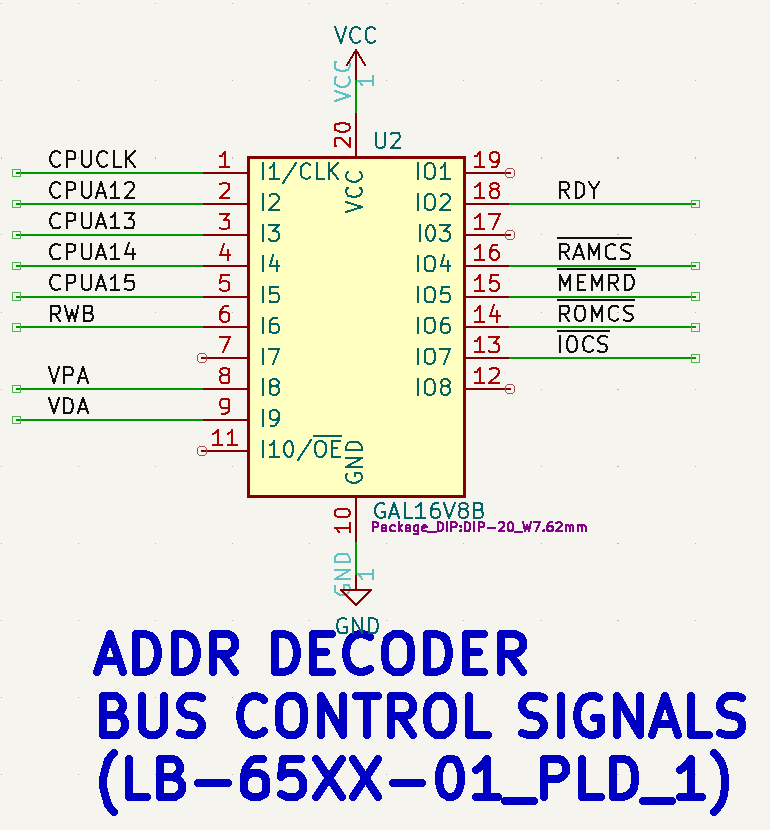
- Address decoder PLD drives RAM/ROM/IO chip selects
- 100x50mm card
Design
PLD
Name       LB-65CXX-01_PLD;
Partno     ATF16V8B;
Date       09/09/20;
Revision   01;
Designer   DOUG G;
Company    LAND BOARDS LLC;
Assembly   U00;
Location   Connellsville, PA;
Device     G16V8;

/*
	65C816 Control
*/


/* Control inputs */
PIN    1   = CLK;
PIN    2   = CPUA12;
PIN    3   = CPUA13;
PIN    4   = CPUA14;
PIN    5   = CPUA15;
PIN    6   = CPUREAD;
PIN    8   = VPA;
PIN    9   = VDA;

/* Counter data inputs */
PIN    13  = !IOCS;
PIN    14  = !ROMCS;
PIN    15  = !MEMRD;
PIN    16  = !RAMCS;
PIN    18  = RDY;

ROMCS = CPUA15 & CPUA14 & CPUA13 & CPUA12 & CPUREAD & VDA
#       CPUA15 & CPUA14 & CPUA13 & CPUA12 & CPUREAD & VPA;

RAMCS = !CPUA15 & VDA
#       !CPUA15 & VPA;

IOCS = CPUA15 & !CPUA14 & !CPUA13 & !CPUA12 & VDA;

MEMRD = CPUREAD & CLK;

/*
RDY = VPA
#     VDA;
*/
