Difference between revisions of "LB-68B50-02"
Jump to navigation
Jump to search
Blwikiadmin (talk | contribs) |
Blwikiadmin (talk | contribs) |
||
| (33 intermediate revisions by the same user not shown) | |||
| Line 1: | Line 1: | ||
| − | [[file:LB-6850- | + | [[file:LB-6850-02_P1090749-720px.jpg]] |
== Features == | == Features == | ||
| Line 12: | Line 12: | ||
== Design == | == Design == | ||
| − | === ACIA | + | === ACIA === |
* 68B50 UART | * 68B50 UART | ||
* Baud Rate Clock (115,200 baud oscillator) | * Baud Rate Clock (115,200 baud oscillator) | ||
| − | [[file:LB-68B50- | + | [[file:LB-68B50-02_ACIA_Rev2.PNG]] |
=== PLD === | === PLD === | ||
* Customize PLD per CPU type and to match memory map | * Customize PLD per CPU type and to match memory map | ||
| − | * ATF16V8B part | + | ** Can be used to support multiple 6850 cards |
| + | * [https://www.mouser.com/ProductDetail/Microchip-Technology/ATF16V8B-15PU?qs=2mdvTlUeTfCsdBIzx6v3gA%3D%3D ATF16V8B] part | ||
* [[TL866ii Plus Programmer]] | * [[TL866ii Plus Programmer]] | ||
| − | [[file:LB-68B50- | + | [[file:LB-68B50-02_U2_PLD_Rev2.PNG]] |
==== LB-68B50-02_6XXX_PLD Listing ==== | ==== LB-68B50-02_6XXX_PLD Listing ==== | ||
| Line 137: | Line 138: | ||
=== Backplane === | === Backplane === | ||
| − | [[file:LB-68B50- | + | [[file:LB-68B50-02_J1_Backplane_Rev2.PNG]] |
== Mechanicals == | == Mechanicals == | ||
| + | |||
| + | === Rev 2 === | ||
[[file:LB-68B50-02_Rev2_MECHS.PNG]] | [[file:LB-68B50-02_Rev2_MECHS.PNG]] | ||
| Line 148: | Line 151: | ||
== Checkout == | == Checkout == | ||
| + | |||
| + | === Rev 2 Checkout === | ||
| + | |||
=== Rev 2 Changes === | === Rev 2 Changes === | ||
| Line 155: | Line 161: | ||
** Inv on one end but not on the other end on schematic | ** Inv on one end but not on the other end on schematic | ||
* Added config jumper J3 into PLD (U2-14) to allow for 2 configs | * Added config jumper J3 into PLD (U2-14) to allow for 2 configs | ||
| − | ** 6502, 6802, 6809 removed | + | ** [[LB-65CXX-01|6502]], [[LB-6802-01|6802]], [[LB-6809-01|6809]] jumper removed |
| − | ** Z80 installed | + | ** [[LB-Z80-01|Z80]] jumper installed |
* Add LED with resistor to U2-15 | * Add LED with resistor to U2-15 | ||
| + | * Moved Osc down a bit | ||
[[file:LB-6850-02_FRONT_REV2(BLK).png]] | [[file:LB-6850-02_FRONT_REV2(BLK).png]] | ||
| − | === Rev 1 === | + | === Rev 1 Checkout === |
| + | |||
| + | ==== IOCS* is on wrong pin ==== | ||
| + | |||
| + | * It is on J1-38 on the Rev 1 PCB | ||
| + | * IOCS* should be on pin J1-37 | ||
| + | * Rework | ||
| + | ** Add wire J1-37 to U2-13 | ||
| + | ** Cut trace near J1-38 | ||
| − | [[file:LB- | + | [[file:LB-68B50-02_J1-38_Rework.PNG]] |
| − | * | + | * Rev 1 before |
| − | |||
| − | |||
| − | |||
[[file:LB-68B50-02_NP_Errors-Rev2.PNG]] | [[file:LB-68B50-02_NP_Errors-Rev2.PNG]] | ||
| − | + | * Fixed on Rev 2 PCB | |
[[file:LB-68B50-02_NP_Fixed-Rev2.PNG]] | [[file:LB-68B50-02_NP_Fixed-Rev2.PNG]] | ||
| + | |||
| + | ==== Missing IORQ signal ==== | ||
| + | |||
| + | * Inverted on one end but not on the other end on schematic | ||
| + | * Rev 1 | ||
| + | |||
| + | [[file:LB-68B50-02_U2_IORQ_Before.PNG]] | ||
| + | |||
| + | * Rev 2 | ||
| + | |||
| + | [[file:LB-68B50-02_U2_IORQ_After.PNG]] | ||
| + | |||
| + | * Rework | ||
| + | ** Add wire U2-13 to J1-51 (Z80) | ||
== Mechanicals == | == Mechanicals == | ||
Latest revision as of 13:55, 16 October 2024
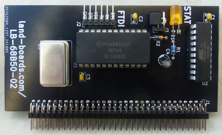
Features
- Serial/Parallel I/O Card
- 68B50 UART
- 1.8432 MHz oscillator
- Baud Rate Clock (115,200 baud oscillator)
- Control PLD
- 100x50mm card
Design
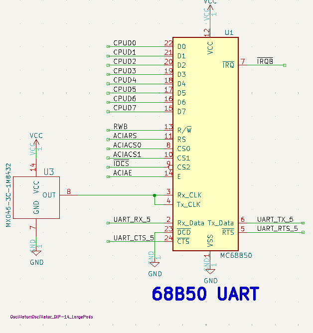
ACIA
- 68B50 UART
- Baud Rate Clock (115,200 baud oscillator)
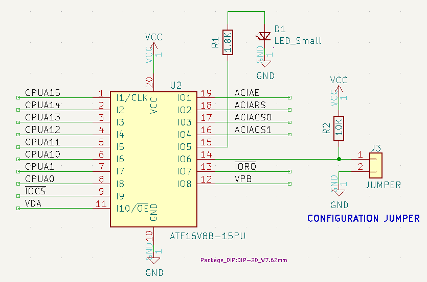
PLD
- Customize PLD per CPU type and to match memory map
- Can be used to support multiple 6850 cards
- ATF16V8B part
- TL866ii Plus Programmer
LB-68B50-02_6XXX_PLD Listing
- 6XXX (6502, 6802, 6809 specific)
Name       LB-68B50-02_6XXX_PLD;
Partno     ATF16V8B;
Date       09/20/24;
Revision   01;
Designer   DOUG G;
Company    LAND BOARDS LLC;
Assembly   LB-68B50-02_6XXX_U2;
Location   Rustbelt, US;
Device     G16V8;

/*
	68B50 Control for LB-6809-01, LB-6802-01, and LB-65CXX CPU boards
	0x8000-0xBFFF - 16KB I/O space
*/

/* Control inputs */
PIN    1   = CPUA15;
PIN    2   = CPUA14;
PIN    3   = CPUA13;
PIN    4   = CPUA12;
PIN    5   = CPUA11;
PIN    6   = CPUA10;
PIN    7   = CPUA1;
PIN    8   = CPUA0;
PIN    9   = !IOCS;	/* IOCS is IO space decoded on all CPU cards 	*/
PIN    11   = VDA;	/* Not used in any version	*/
PIN    12   = VPB;	/* VPB is enable on 6802, 6809 AND 6502 (Rev 2 rwk) CPUs */
PIN    14   = !IORQ;	/* IORQ* is enable on Z80 cards	*/

/* Address Decode and Chip Select outputs */
PIN    16  = ACIACS1;
PIN    17  = ACIACS0;
PIN    18  = ACIARS;
PIN    19  = ACIAE;

ACIACS1 = CPUA15 & !CPUA14 & IOCS;

ACIACS0 = CPUA15 & !CPUA14 & IOCS;

ACIARS = CPUA0;

ACIAE = CPUA15 & !CPUA14 & IOCS & VPB;
LB-68B50-02_Z80_PLD PLD Listing
Name       LB-68B50-02_Z80_PLD;
Partno     ATF16V8B;
Date       09/19/24;
Revision   01;
Designer   DOUG G;
Company    LAND BOARDS LLC;
Assembly   LB-6850-02_U2;
Location   Rustbelt, US;
Device     G16V8;

/*
	68B50 Control for Z80 CPU board
*/

/* Control inputs */
PIN    1   = CPUA15;
PIN    2   = CPUA14;
PIN    3   = CPUA13;
PIN    4   = CPUA12;
PIN    5   = CPUA11;
PIN    6   = CPUA10;
PIN    7   = CPUA1;
PIN    8   = CPUA0;
PIN    9   = !IOCS;
PIN    11  = VDA;
PIN    12  = VPB;
PIN    13  = !IORQ;

/* Address Decode and Chip Select outputs */
PIN    16  = ACIACS1;
PIN    17  = ACIACS0;
PIN    18  = ACIARS;
PIN    19  = ACIAE;

ACIACS1 = IOCS & IORQ;

ACIACS0 = IOCS & IORQ;

ACIARS = CPUA0;

ACIAE = IOCS & IORQ;
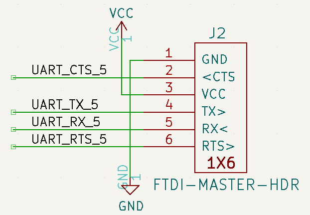
J2 - FTDI Header)
- 5V levels
- Pinout
- GND
- CTS (in)
- VCC
- TX (out)
- RX (in)
- RTS (out)
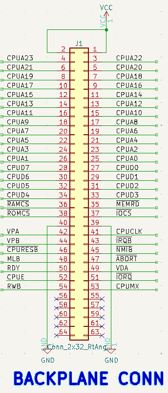
Backplane
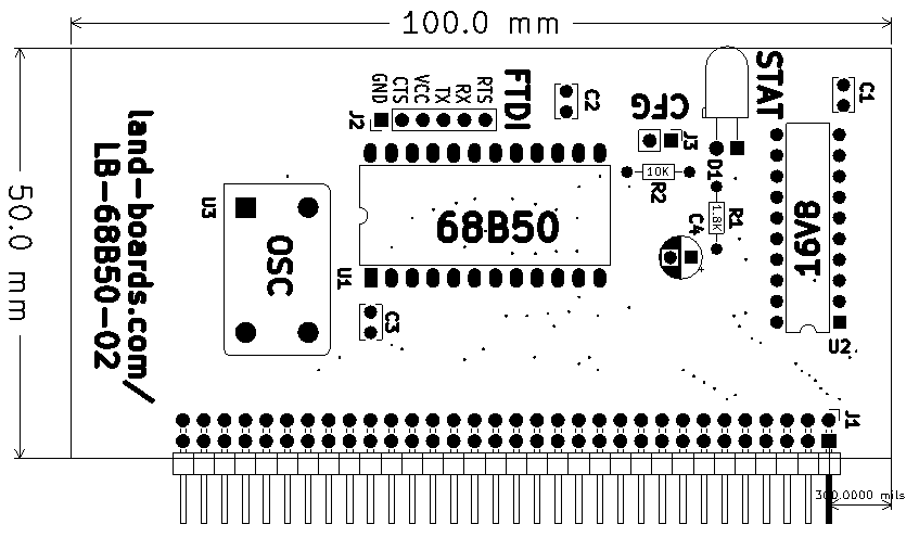
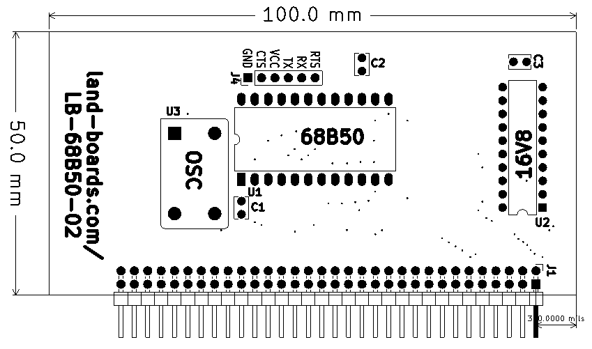
Mechanicals
Rev 2
Rev 1
Checkout
Rev 2 Checkout
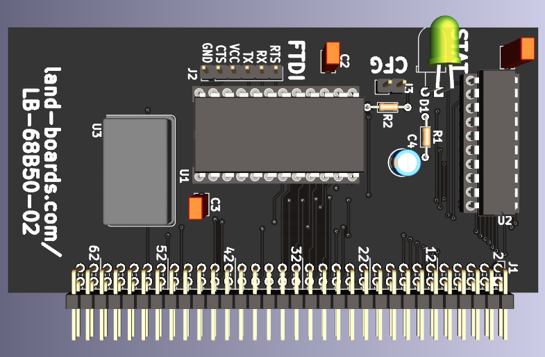
Rev 2 Changes
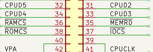
- Fixed IOCS* to be on J1-38
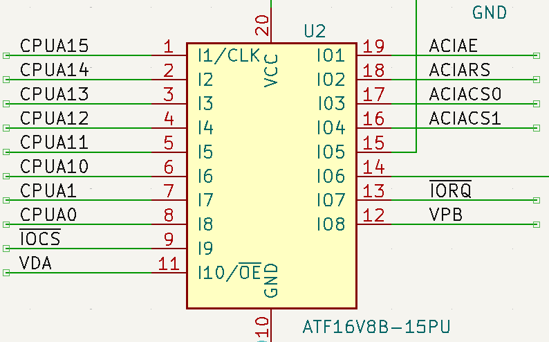
- Fixed IORQ signal
- Inv on one end but not on the other end on schematic
- Added config jumper J3 into PLD (U2-14) to allow for 2 configs
- Add LED with resistor to U2-15
- Moved Osc down a bit
Rev 1 Checkout
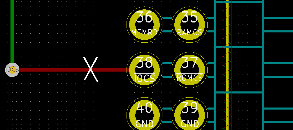
IOCS* is on wrong pin
- It is on J1-38 on the Rev 1 PCB
- IOCS* should be on pin J1-37
- Rework
- Add wire J1-37 to U2-13
- Cut trace near J1-38
- Rev 1 before
- Fixed on Rev 2 PCB
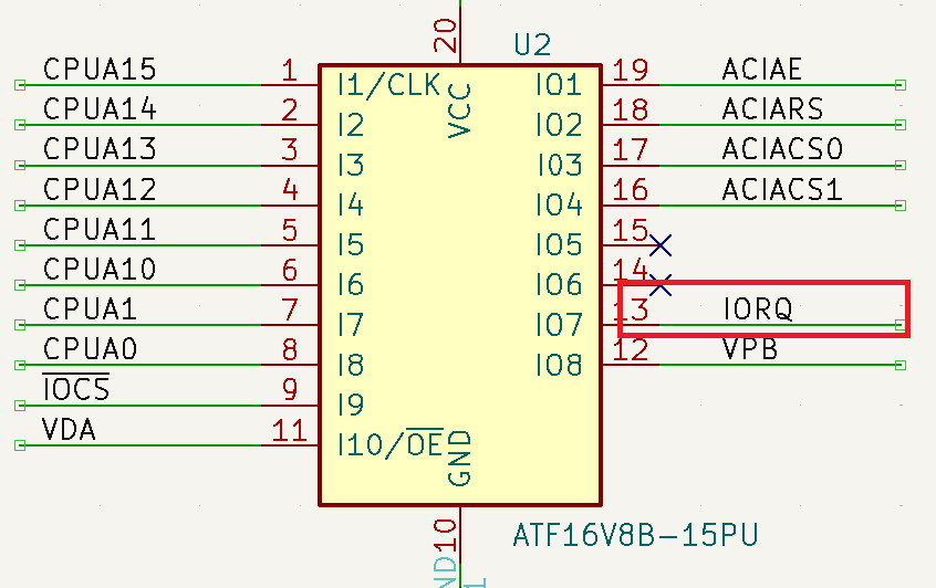
Missing IORQ signal
- Inverted on one end but not on the other end on schematic
- Rev 1
- Rev 2
- Rework
- Add wire U2-13 to J1-51 (Z80)
