Difference between revisions of "RETRO-EP4CE15"
Jump to navigation
Jump to search
Blwikiadmin (talk | contribs) |
Blwikiadmin (talk | contribs) |
||
| Line 293: | Line 293: | ||
=== J3 Header (EP4CE15/EP4CE55 FPGA pin numbers) === | === J3 Header (EP4CE15/EP4CE55 FPGA pin numbers) === | ||
| − | * J8P55 = | + | * J8P55 = Pin_B22 |
| − | * J8P56 = | + | * J8P56 = Pin_B21 |
| − | * J8B57 = | + | * J8B57 = Pin_N20 |
| − | * J8P58 = | + | * J8P58 = Pin_N19 |
| − | * J8P59 = | + | * J8P59 = Pin_M20 |
| − | * J8P60 = | + | * J8P60 = Pin_M19 |
=== J3 Header (5CEFA2F23/5CEF52F23 FPGA Card pin numbers) === | === J3 Header (5CEFA2F23/5CEF52F23 FPGA Card pin numbers) === | ||
Revision as of 13:50, 16 June 2021
Contents
- 1 Features
- 2 FPGA Boards
- 3 SRAM
- 4 SDRAM 16MB X 16
- 5 Connectors
- 6 Headers/Jumpers
- 7 VGA - Ideal Drive 2:2:2 Case
- 8 Schematic
- 9 Programming the FPGA EEPROM
- 10 FPGA Retrocomputer Builds
- 11 Testing the Interfaces on the card
- 12 Checkout
- 13 Comment out SDRAM if unused
- 14 Pin List
- 15 Assembly Sheet
Features
- Full MultiComp Support of classic 8-bit Retrocomputers
- Other builds
- Supports Cyclone IV or Cyclone V FPGA Cards by QMTECH
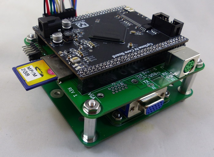
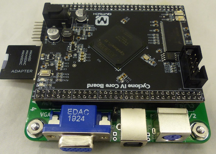
- EP4CE15 Cyclone IV FPGA Card (tested)
- EP4CE55 Cyclone IV FPGA Card (untested)
- 5CEFA2F23 Cyclone V FPGA Card (tested)
- 5CEFA5F23 Cyclone V FPGA Card (untested)
- 1MB SRAM
- IS62WV10248EBLL-45TLI, SRAM. Async, 1Mbx8, 45ns
- For banked use in CP/M and as RAM Disk in other 8-bit micro designs
- VGA connector
- 6 bit video (2:2:2)
- PS/2 connector
- FTDI USB to serial converter
- Genuine FT230XS FTDI USB to Serial chip
- USB B
- Tx/Rx LEDs
- SD or SDHC Card
- Can do micro SDHC card using SD card adapter
- 2x6 Header
- Power card from either FPGA card connector or USB power
- 50-pin I/O Connector
- 95x95mm form factor card
- 4x 6-32 mounting holes
- Low Profile
FPGA Boards
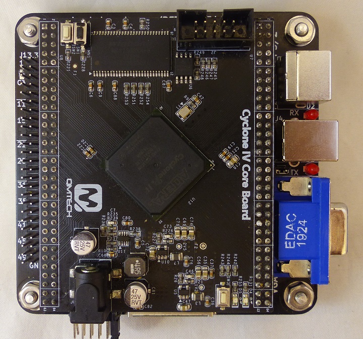
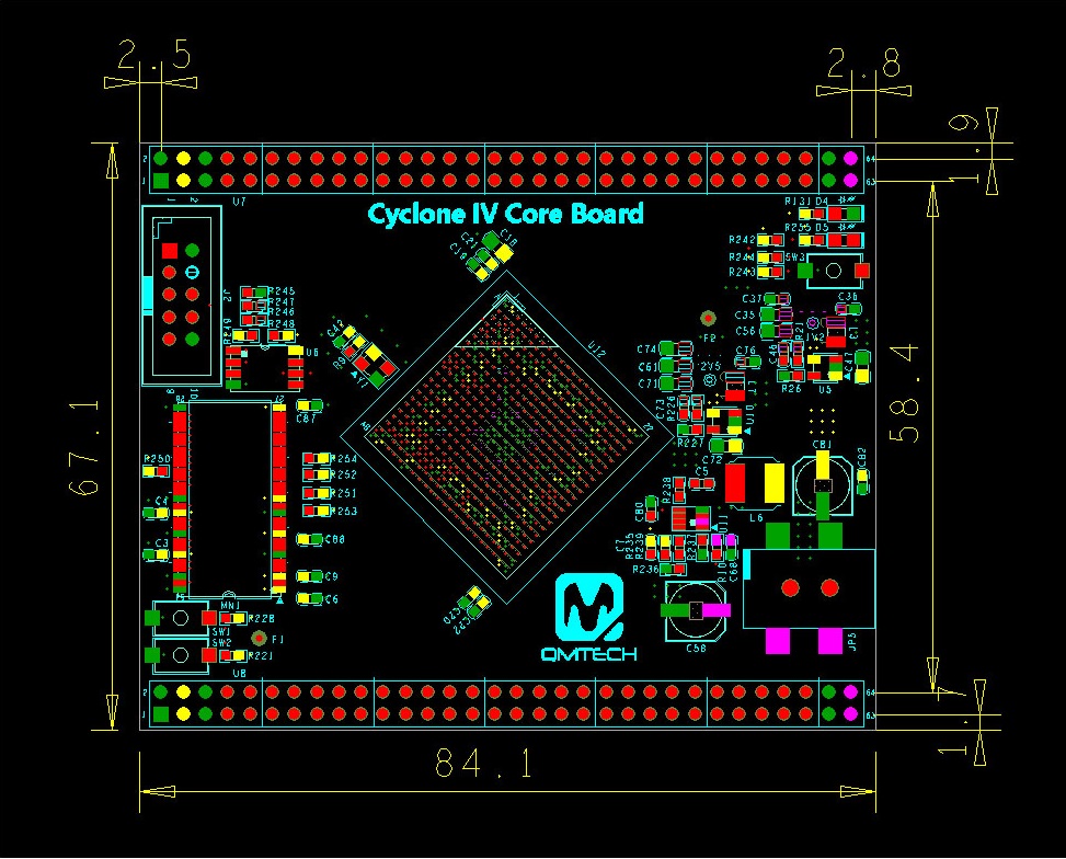
QMTECH EP4CE15
- QMTECH EP4CE15 Board
- AliExpress listing FPGA Card
- Altera Cyclone IV EP4CE15F23C8N FPGA
- 32MB SDRAM
- 32MB SDRAM, W9825C6KH-6 Winbond 4M X 4 Banks x 16 bits SDRAM
- 15K logic cells
- Crystal frequency: 50 MHz
- 3 Switches
- 2 LEDs
- Power supply
- 1A@5V DC, the DC header type: DC-050, 5.5mmx2.1mm
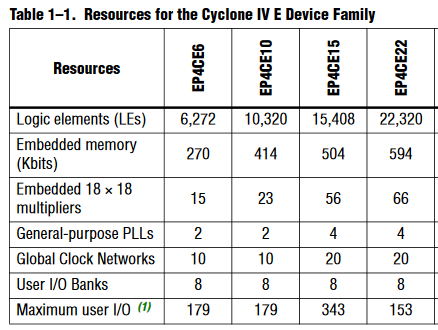
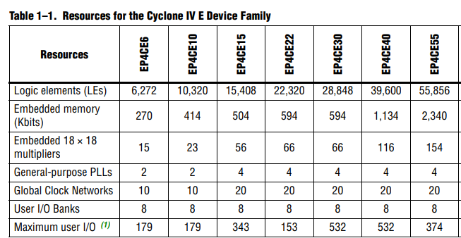
Cyclone IV EP4CE15 FPGA Resources
- 56 1Kx9 RAM blocks
EP4CE15 Card Resources
- Power LED - D4
- User LED - D5 - FPGA Pin_E4 (pull low to illuminate LED)
- KEY0 - SW1 - FPGA Pin_W13
- KEY1 - SW2 - FPGA Pin_Y13
- nCONFIG - SW3 = FPGA Pin_K5
- CLK_50M = FPGA Pin_T2
- JP5 - 5V
QMTECH EP4CE55
- QMTECH EP4CE55 Board
- AliExpress listing FPGA Card
- Altera Cyclone IV EP4CE55F23C8N FPGA
- 32MB SDRAM
- 55K logic cells
- 2.3Mbits internal SRAM
- Crystal frequency: 50MHz
- 3 Switches
- 2 LEDs
- Power supply
- 1A@5V DC, the DC header type: DC-050, 5.5mmx2.1mm
Cyclone IV EP4CE55 FPGA Resources
- 260 1Kx9 RAM blocks
- Power LED - D4
- User LED - D5 - FPGA Pin_E4 (pull low to illuminate LED)
- KEY0 - SW1 - FPGA Pin_W13
- KEY1 - SW2 - FPGA Pin_Y13
- nCONFIG - SW3
- JP5 - 5V
EP4CE55 Card Mechanicals
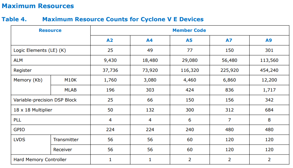
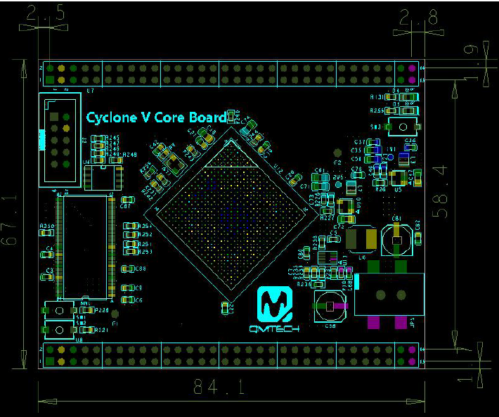
QMTECH 5CEFA2F23 FPGA Board
- QMTech Cyclone V FPGA Board
- AliExpress listing QMTECH Altera Intel FPGA Core Board Cyclone V 5CEFA2F23 SDRAM
- Altera Cyclone V 5CEFA2F23 FPGA
- On-Board crystal frequency 50MHz
- RAM resource up to 1,760Kb
- 176 blocks of 1Kx10
- 25K logic cells
- Micron MT25QL128A SPI Flash, 16M bytes for user configuration code
- 32MB SDRAM, W9825C6KH-6 Winbond 4M X 4 Banks x 16 bits SDRAM
- 3.3V power supply for FPGA by using MP2315 wide input range DC/DC
- 5CEFA2F23 core board has two 64p, 2.54mm pitch headers
- 3 user switches
- 2 user LEDs
- Default power source for board is: 1A@5V DC, the DC header type: DC-050, 5.5mmx2.1mm
Cyclone V_FPGA Resources
- 176 1Kx10 RAM blocks
- Power LED - D4 (On when 5V is applied)
- User LED - LED_D5 - FPGA Pin_D17 (pull low to illuminate LED)
- KEY0 - SW1 - FPGA Pin_AB13
- RESET_N- SW2 - FPGA PIN_V18
- nCONFIG - SW3 - FPGA PIN_A4
- JP5 - 5V
5CEFA2F23 Card Mechanicals
QMTECH 5CEFA5F23 FPGA Board
- QMTech Cyclone V FPGA Board
- AliExpress listing QMTECH Altera Intel FPGA Core Board Cyclone V 5CEFA5F23 SDRAM
- Altera Cyclone V 5CEFA5F23 FPGA
- On-Board crystal frequency 50MHz
- RAM resource up to 4.460Kb
- 77K logic cells
- Micron MT25QL128A SPI Flash, 32M bytes for user configuration code
- 2x 32MB SDRAM, Winbond W9825G6KH-6
- 3.3V power supply for FPGA by using MP2315 wide input range DC/DC
- 5CEFA5F23 core board has two 64p, 2.54mm pitch headers
- 3 user switches
- 2 user LEDs
- Default power source for board is: 1A@5V DC, the DC header type: DC-050, 5.5mmx2.1mm
Cyclone V 5CEFA5F23 FPGA Resources
- 446 1Kx10 RAM blocks
- Power LED - D4 (On when 5V is applied)
- User LED - LED_D5 - FPGA Pin_D17 (pull low to illuminate LED)
- KEY0 - SW1 - FPGA Pin_AB13
- RESET_N- SW2 - FPGA PIN_V18
- nCONFIG - SW3 - FPGA PIN_A4
- JP5 - 5V
5CEFA5F23 Card Mechanicals
SRAM
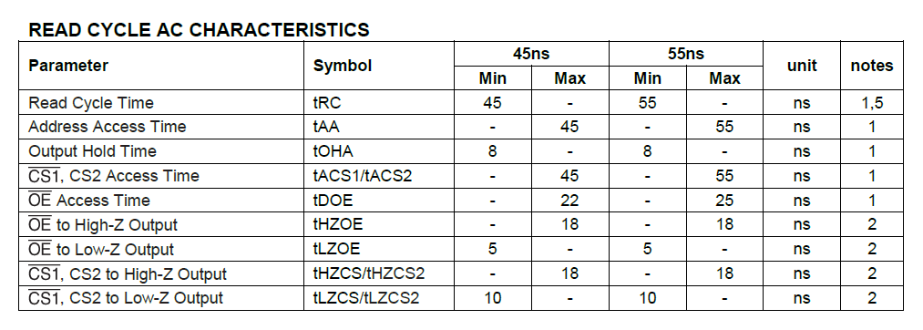
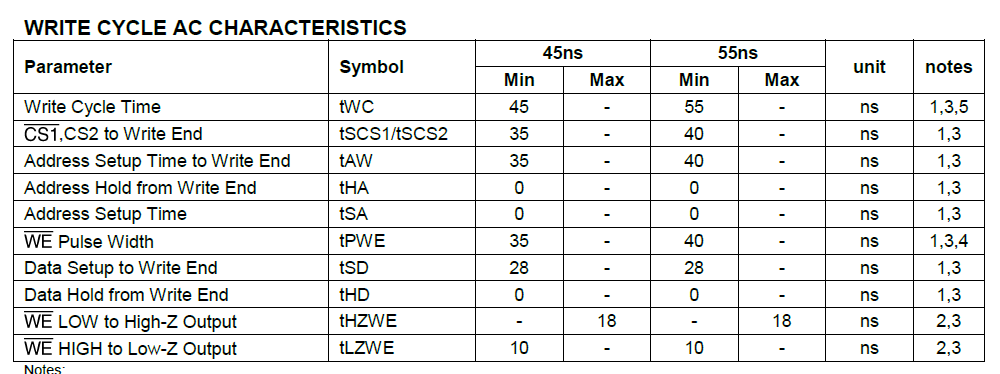
- IS62WV10248EBLL-45TLI, SRAM. Async, 1Mbx8, 45ns
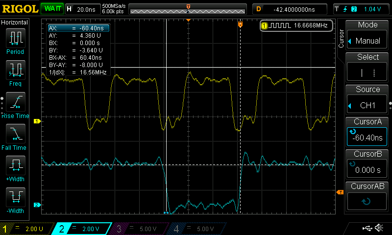
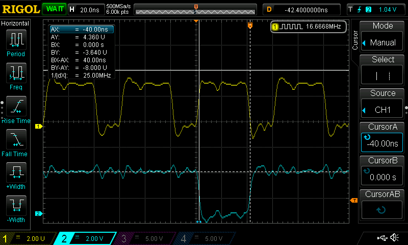
Read Timing
- CPU at 16.7 MHz
- 2/1 clocks of 50 MHz
- Yellow = CPU clk
- Cyan = SRAM_OE
Write Timing
- CPU at 16.7 MHz
- 2/1 clocks of 50 MHz
- Yellow = CPU clk
- Cyan = SRAM_WE
SRAM (EP4CE15/EP4CE55 FPGA pin numbers) J7 - U7
- n_sRamCS - J7-19 - PIN_F1
- n_sRamWE - J7-29 - PIN_B4
- n_sRamOE - J7-16 - PIN_J2
- sramData[0] - J7-21 - PIN_E1
- sramData[1] - J7-23 - PIN_C1
- sramData[2] - J7-25 - PIN_B1
- sramData[3] - J7-27 - PIN_B3
- sramData[4] - J7-26 - PIN_B2
- sramData[5] - J7-24 - PIN_C2
- sramData[6] - J7-22 - PIN_D2
- sramData[7] - J7-20 - PIN_F2
- sramAddress[0] - J7-17 - PIN_H1
- sramAddress[1] - J7-15 - PIN_J1
- sramAddress[2] - J7-13 - PIN_M1
- sramAddress[3] - J7-11 - PIN_N1
- sramAddress[4] - J7-9 - PIN_P1
- sramAddress[5] - J7-10 - PIN_P2
- sramAddress[6] - J7-12 - PIN_N2
- sramAddress[7] - J7-14 - PIN_M2
- sramAddress[8] - J7-18 - PIN_H2
- sramAddress[9] - J7-28 - PIN_A3
- sramAddress[10] - J7-30 - PIN_A4
- sramAddress[11] - J7-32 - PIN_C3
- sramAddress[12] - J7-34 - PIN_A5
- sramAddress[13] - J7-36 - PIN_A6
- sramAddress[14] - J7-38 - PIN_A7
- sramAddress[15] - J7-40 - PIN_A8
- sramAddress[16] - J7-37 - PIN_B7
- sramAddress[17] - J7-35 - PIN_B6
- sramAddress[18] - J7-33 - PIN_B5
- sramAddress[19] - J7-31 - PIN_C4
SRAM (5CEFA2F23/5CEFA5F23 FPGA pin numbers) J7 - U7
- n_sRamCS - J7-19 - PIN_E2
- n_sRamWE - J7-29 - PIN_D6
- n_sRamOE - J7-16 - PIN_L2
- sramData[0] - J7-21 - PIN_C1
- sramData[1] - J7-23 - PIN_G6
- sramData[2] - J7-25 - PIN_G8
- sramData[3] - J7-27 - PIN_F7
- sramData[4] - J7-26 - PIN_H8
- sramData[5] - J7-24 - PIN_H6
- sramData[6] - J7-22 - PIN_C2
- sramData[7] - J7-20 - PIN_D3
- sramAddress[0] - J7-17 - PIN_G1
- sramAddress[1] - J7-15 - PIN_L1
- sramAddress[2] - J7-13 - PIN_N1
- sramAddress[3] - J7-11 - PIN_U1
- sramAddress[4] - J7-9 - PIN_Y3
- sramAddress[5] - J7-10 - PIN_W2
- sramAddress[6] - J7-12 - PIN_U2
- sramAddress[7] - J7-14 - PIN_N2
- sramAddress[8] - J7-18 - PIN_G2
- sramAddress[9] - J7-28 - PIN_E7
- sramAddress[10] - J7-30 - PIN_C6
- sramAddress[11] - J7-32 - PIN_D9
- sramAddress[12] - J7-34 - PIN_A5
- sramAddress[13] - J7-36 - PIN_B7
- sramAddress[14] - J7-38 - PIN_A8
- sramAddress[15] - J7-40 - PIN_A10
- sramAddress[16] - J7-37 - PIN_A7
- sramAddress[17] - J7-35 - PIN_B6
- sramAddress[18] - J7-33 - PIN_B5
- sramAddress[19] - J7-31 - PIN_E9
SDRAM 16MB X 16
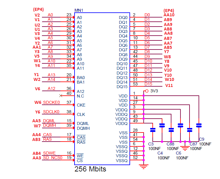
EP4 SDRAM
- W9825C6KH-6 Winbond 4M X 4 Banks x 16 bits SDRAM
- 13 rows, 9 columns
Connectors
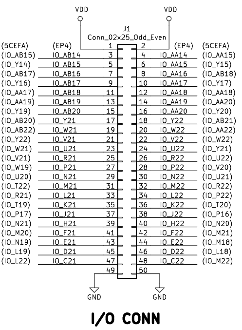
J1 - I/O Connector
(5CEFA2F23 FPGA Card pin numbers in parenthesis)
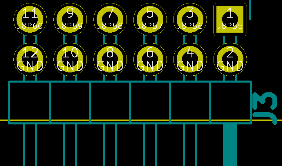
J3 - Edge I/O Connector
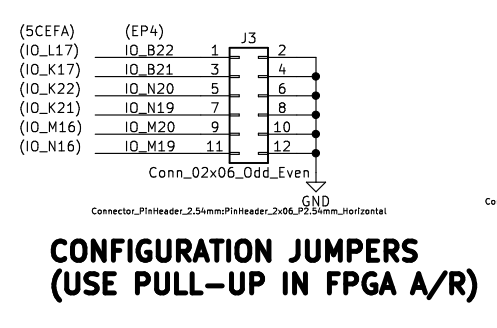
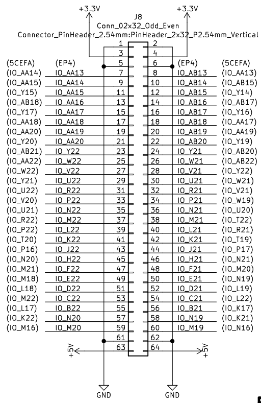
J3 Header (EP4CE15/EP4CE55 FPGA pin numbers)
- J8P55 = Pin_B22
- J8P56 = Pin_B21
- J8B57 = Pin_N20
- J8P58 = Pin_N19
- J8P59 = Pin_M20
- J8P60 = Pin_M19
J3 Header (5CEFA2F23/5CEF52F23 FPGA Card pin numbers)
- J8P55 = BANK_5B_L17
- J8P56 = BANK_5B_K17
- J8B57 = BANK_5B_K22
- J8P58 = BANK_5B_K21
- J8P59 = BANK_5N_M16
- J8P60 = BANK_5B_N16
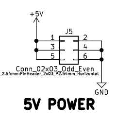
J5 Power
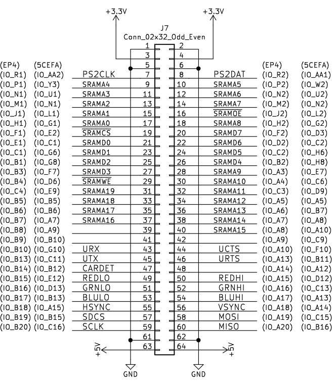
J7 Pin Mapping Card to FPGA pins - Right connector
- These are the connections to the VGA, PS/2, Serial, SRAM, etc
- Both the EP4 and 5F FPGA cards have the same connectors but they go to different FPGA pins
- This is the mapping between the two cards
- EP4 is the Cyclone IV card
- 5CEFA is the Cyclone V card
- This is the mapping between the two cards
J8 Pin Mapping Card to FPGA pins - Left connector
Headers/Jumpers
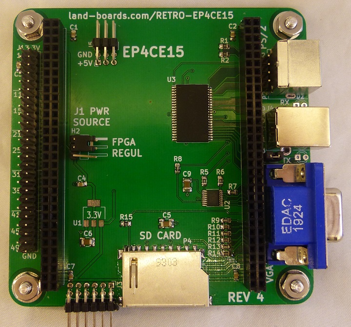
H1 - Power
- Install jumper to power card from USB 5V
- Do not apply power to FPGA DC jack when this jumper is installed
H2 - I/O Power Source for J1
- 1-2 = FPGA 3.3V Power
- 2-3 = On-board 3.3V Regulator
P1 - (2:2:2) VGA
P1 - VGA (EP4CE15 Card)
- videoR0 = U7-49 = PIN_B15
- videoR1 = U7-50 = PIN_A15
- videoG0 = U7-51 = PIN_B16
- videoG1 = U7-52 = PIN_A16
- videoB0 = U7-53 = PIN_B17
- videoB1 = U7-54 = PIN_A17
- hSync = U7-55 = PIN_B18
- vSync = U7-56 = PIN_A18
P1 - VGA (5CEFA2F23 Card)
- videoR0 = U8-49 = PIN_E12
- videoR1 = U8-50 = PIN_D12
- videoG0 = U8-51 = PIN_D13
- videoG1 = U8-52 = PIN_C13
- videoB0 = U8-53 = PIN_B13
- videoB1 = U8-54 = PIN_A13
- hSync = U8-55 = PIN_A15
- vSync = U8-56 = PIN_A14
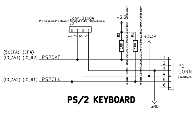
P2 - PS/2 Keyboard
- Not every PS/2 keyboard works at 3.3V but many do
- P2 - PS/2 Keyboard (EP4CE15 FPGA pin numbers)
- PS2DAT = U7-8 = PIN_R2
- PS2CLK = U7-8 = PIN_R1
P2 - PS/2 Keyboard (5CEFA2F23 FPGA Card pin numbers)
- PS2DAT = U7-8 = PIN_BANK_2A_AA1
- PS2CLK = U7-8 = PIN_NANK_2A_AA2
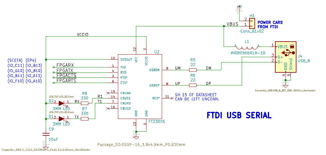
P3 - USB/Serial Port
- USB-B MICRO (Rev 1-3) or Full Sized B (Rev 4)
P3 - USB-B (EP4CE15 FPGA pin numbers)
- FT230X FTDI USB to Serial
- serSelect = U8-55 = PIN_B22 (J3-1 TO -2)
- Needs weak pullup
- set_instance_assignment -name WEAK_PULL_UP_RESISTOR ON -to serSelect
- Needs weak pullup
- txd1 = U7-43 = PIN_B10
- rxd1 = U7-45 = PIN_B13
- Needs weak pullup
- set_instance_assignment -name WEAK_PULL_UP_RESISTOR ON -to rxd1
- Needs weak pullup
- rts1 = U7-44 = PIN_A10
- cts1 = U7-46 = PIN_A13
P3 - USB-B B (5CEFA2F23 FPGA Card pin numbers)
- FT230X FTDI USB to Serial
- serSelect = U8-55 = PIN_L17 (J3-1 TO -2)
- Needs weak pullup
- set_instance_assignment -name WEAK_PULL_UP_RESISTOR ON -to serSelect
- Needs weak pullup
- txd1 = U7-43 = PIN_G10
- rxd1 = U7-45 = PIN_C11
- Needs weak pullup
- set_instance_assignment -name WEAK_PULL_UP_RESISTOR ON -to rxd1
- Needs weak pullup
- rts1 = U7-44 = PIN_F10
- cts1 = U7-46 = PIN_B11
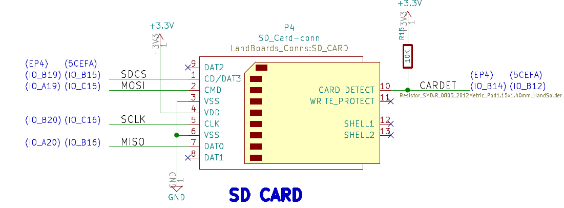
P4 - SD Card
P4 - SD Card (5CEFA2F23 FPGA pin numbers)
- SDCS = U7-57 = PIN_BANK_7A_B15
- MOSI = U7-58 = PIN_BANK_7A_C15
- SCK = U7-59 = PIN_BANK_7A_C16
- MISO = U7-60 = PIN_BANK_7A_B16
- SD_DETECT - PIN_B12
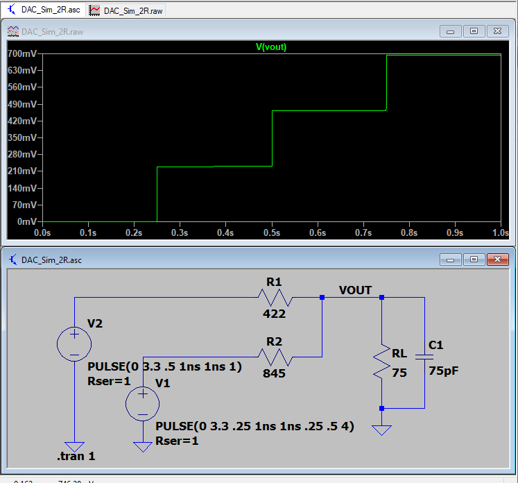
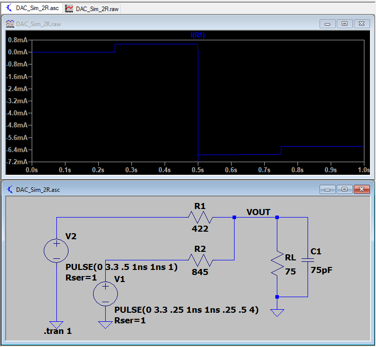
VGA - Ideal Drive 2:2:2 Case
- FPGA has a 3.3V driver which can drive 8 mA
- Ideal case drive current
- 0.7V into 75 Ohms = 9.33 mA
- R-2R values
- Ideal resistor values are 417.9 ohms and 835.7 ohms
- Standard value 1% resistors
- 1% standard values are 422 (Mouser), 845 (Mouser) Ohms
- Get closest values
- 0V, 0.228V, 0.460V, 0.693V
- Voltage steps are:
- Current steps are:
Schematic
Programming the FPGA EEPROM
Programming the FPGA EEPROM (EP4CE15)
- File
- Convert Programming File
- Configuration Device = EPCQ64
- Mode = Active Serial
- Programming File Type: *.jic
- Advanced = Check both Disables...
- Select Flash Loader
- Add Device = Cyclone IV E and EP4CE15
- Select SOF Data
- Select Add File and select the .sof file
- Generate
- In Tools, Programmer
- Mode: JTAG
- Add file and select the .jic file
- Select Program/Configure
- Takes a while to program
- Press button near VGA
Programming the FPGA EEPROM (5CEFA2F23 FPGA)
- File
- Convert Programming File
- Configuration Device = MT25QL128
- Mode = Active Serial
- Programming File Type: *.jic
- Advanced = Check both Disables...
- Select Flash Loader
- Add Device = Cyclone V and 5CEFA2
- Select SOF Data
- Select Add File and select the .sof file
- Generate
- In Tools, Programmer
- Mode: JTAG
- Add file and select the .jic file
- Select Program/Configure
- Takes a while to program
- Press button near VGA
FPGA Retrocomputer Builds
Testing the Interfaces on the card
Here's a way to test the interfaces on the card, including the 1MB SRAM.
- Requires
- VGA display
- PS/2 keyboard
- Host PC running PuTTY over the USB-serial interface
- FPGA build - OSI M6502 VGA Multicomp - VHDL code - Build/Load to FPGA
- 40KB Internal SRAM used by BASIC
- 1MB External SRAM banked as 128 banks of 8KB in the M6502 space
- Bank select register at 0xFFD4
- 6502 address space from 0xC000-0xDFFF
- Load RAM Test BASIC program - Loads/runs under OSI M6502 Multicomp build
- Test the Bank Register works by incrementing the register filling the first location with the bank number and verifying all writes worked
- Tests single 8K
- Between these two tests checks all data, address and control lines to the External SRAM
- Steps to load/run
- Run FPGA code and hit enter on PS/2 keyboard until power on tests are done and BASIC prompt is on VGA
- Open BASIC program BANKTST2.BAS (above) in text editor
- Run Serial port run terminal emulator, like PuTTY
- On PS/2 keyboard, Press F1 to select serial port instead of VGA
- Copy BASIC program (Ctrl-A, Ctrl-C) to copy/paste buffer
- Paste into PuTTY (right click in PuTTY window)
- Type "RUN" on PuTTY terminal
- Result will be printed to the screen
- Runs fairly quickly, the OSI M6502 is a 12.5 MHz design (slowed down for external SRAM)
Checkout
Rev 4 Issues
- Built and tested, no issues
Rev 2 Issues
- GND on wrong USB pin
- Was pin 4, s/b pin 5
- Cut etch J4-4 to via
- Add wire J4-5 to via
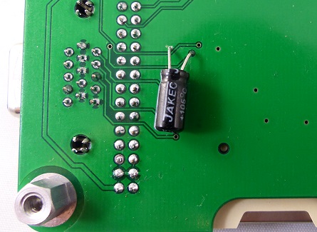
- FT230XS +3.3V out needs 10 uF cap (min)
- Added 47uF electrolytic cap between via GND and vusb (3.3V) on rear of board
Rev 1 Issues
- Wrong DB15HD footprint
- Change to right footprint in Rev 2
- USB-C too hard to hand solder
- Changing to USB-B Micro in Rev 2
- Add 5V header in Rev 2
Rev 1 Prototype
- VGA connector footprint problem
- Using the J1 connector to VGAX49 card
| Signal | VGAX49 Pin | RETRO Pin | FPGA Pin |
|---|---|---|---|
| GND | J1-19 | J1-49 | N/A |
| R4 | J1-1 | J1-47 | C21 |
| R3 | J1-2 | J1-48 | C22 |
| G5 | J1-6 | J1-45 | D21 |
| G4 | J1-7 | J1-46 | D22 |
| B4 | J1-12 | J1-43 | E21 |
| B3 | J1-13 | J1-44 | E22 |
| HS | J1-17 | J1-41 | F21 |
| VS | J1-18 | J1-42 | F22 |
- Serial
| Signal | RETRO Pin | FPGA Pin |
|---|---|---|
| GND | J1-50 | N/A |
| SerTx | J1-39 | H21 |
| SerRx | J1-40 | H22 |
| SerCts | J1-37 | J21 |
| SerRts | J1-38 | J22 |
Testing with R32V2020 and Multicomp
- VGA (on P1 to VGAX49 Card) works
- Mounted on CARRIER95TO49MM board
- PS/2 Keyboard connector on RETRO-EP4CE15 works
- Installed R1, R2 - 10K pull-ups
- R32V2020 - Land Boards 32-bit RISC CPU Works
- 40K SRAM, BASIC UK101 worked
- External SRAM works - Tested 40KB
- CP/M tested - Works with SD Card
- Running ZEXALL
- Wrong color Mini-DIN (keyboard s/b purple)
Comment out SDRAM if unused
- Insert into entity at top
-- Not using the SD RAM but making sure that it's not active
n_sdRamCas	: out std_logic := '1';		-- CAS on schematic
n_sdRamRas	: out std_logic := '1';		-- RAS
n_sdRamWe	: out std_logic := '1';		-- SDWE
n_sdRamCe	: out std_logic := '1';		-- SD_NCS0
sdRamClk		: out std_logic := '1';		-- SDCLK0
sdRamClkEn	: out std_logic := '1';		-- SDCKE0
sdRamAddr	: out std_logic_vector(14 downto 0) := "000"&x"000";
sdRamData	: in std_logic_vector(15 downto 0);
Pin List
Pin List (EP4CE15)
set_global_assignment -name FAMILY "Cyclone IV E"
set_global_assignment -name DEVICE EP4CE15F23C8
set_global_assignment -name TOP_LEVEL_ENTITY Microcomputer
set_global_assignment -name ORIGINAL_QUARTUS_VERSION "13.0 SP1"
set_global_assignment -name PROJECT_CREATION_TIME_DATE "17:55:48  OCTOBER 20, 2013"
set_global_assignment -name LAST_QUARTUS_VERSION "18.1.0 Lite Edition"
set_global_assignment -name PROJECT_OUTPUT_DIRECTORY output_files
set_global_assignment -name PARTITION_NETLIST_TYPE SOURCE -section_id Top
set_global_assignment -name PARTITION_FITTER_PRESERVATION_LEVEL PLACEMENT_AND_ROUTING -section_id Top
set_global_assignment -name PARTITION_COLOR 16764057 -section_id Top
set_global_assignment -name MIN_CORE_JUNCTION_TEMP 0
set_global_assignment -name MAX_CORE_JUNCTION_TEMP 85
set_global_assignment -name DEVICE_FILTER_PACKAGE FBGA
set_global_assignment -name DEVICE_FILTER_SPEED_GRADE 8
set_global_assignment -name STRATIX_DEVICE_IO_STANDARD "3.3-V LVTTL"
# Clock and reset
set_location_assignment PIN_T2 -to i_CLOCK_50
set_location_assignment PIN_W13 -to n_reset
set_instance_assignment -name WEAK_PULL_UP_RESISTOR ON -to n_reset
# PS/2
set_location_assignment PIN_R1 -to ps2Clk
set_instance_assignment -name WEAK_PULL_UP_RESISTOR ON -to ps2Clk
set_location_assignment PIN_R2 -to ps2Data
set_instance_assignment -name WEAK_PULL_UP_RESISTOR ON -to ps2Data
# Serial
set_location_assignment PIN_B22 -to serSelect
set_instance_assignment -name WEAK_PULL_UP_RESISTOR ON -to serSelect
set_location_assignment PIN_A13 -to cts1
set_instance_assignment -name WEAK_PULL_UP_RESISTOR ON -to cts1
set_location_assignment PIN_A10 -to rts1
set_location_assignment PIN_B13 -to rxd1
set_instance_assignment -name WEAK_PULL_UP_RESISTOR ON -to rxd1
set_location_assignment PIN_B10 -to txd1
# SD Card
set_location_assignment PIN_B19 -to sdCS
set_location_assignment PIN_A19 -to sdMOSI
set_location_assignment PIN_B20 -to sdClock
set_location_assignment PIN_A20 -to sdMISO
set_instance_assignment -name WEAK_PULL_UP_RESISTOR ON -to sdMISO
set_location_assignment PIN_B14 -to sdCardDet_n
set_location_assignment PIN_E4 -to driveLED
# Video
set_location_assignment PIN_B15 -to videoR0
set_location_assignment PIN_A15 -to videoR1
set_location_assignment PIN_B16 -to videoG0
set_location_assignment PIN_A16 -to videoG1
set_location_assignment PIN_B17 -to videoB0
set_location_assignment PIN_A17 -to videoB1
set_location_assignment PIN_B18 -to hSync
set_location_assignment PIN_A18 -to vSync
# SRAM
set_location_assignment PIN_F1 -to n_sRamCS
set_location_assignment PIN_B4 -to n_sRamWE
set_location_assignment PIN_J2 -to n_sRamOE
set_location_assignment PIN_E1 -to sramData[0]
set_location_assignment PIN_C1 -to sramData[1]
set_location_assignment PIN_B1 -to sramData[2]
set_location_assignment PIN_B3 -to sramData[3]
set_location_assignment PIN_B2 -to sramData[4]
set_location_assignment PIN_C2 -to sramData[5]
set_location_assignment PIN_D2 -to sramData[6]
set_location_assignment PIN_F2 -to sramData[7]
set_location_assignment PIN_H1 -to sramAddress[0]
set_location_assignment PIN_J1 -to sramAddress[1]
set_location_assignment PIN_M1 -to sramAddress[2]
set_location_assignment PIN_N1 -to sramAddress[3]
set_location_assignment PIN_P1 -to sramAddress[4]
set_location_assignment PIN_P2 -to sramAddress[5]
set_location_assignment PIN_N2 -to sramAddress[6]
set_location_assignment PIN_M2 -to sramAddress[7]
set_location_assignment PIN_H2 -to sramAddress[8]
set_location_assignment PIN_A3 -to sramAddress[9]
set_location_assignment PIN_A4 -to sramAddress[10]
set_location_assignment PIN_C3 -to sramAddress[11]
set_location_assignment PIN_A5 -to sramAddress[12]
set_location_assignment PIN_A6 -to sramAddress[13]
set_location_assignment PIN_A7 -to sramAddress[14]
set_location_assignment PIN_A8 -to sramAddress[15]
set_location_assignment PIN_B7 -to sramAddress[16]
set_location_assignment PIN_B6 -to sramAddress[17]
set_location_assignment PIN_B5 -to sramAddress[18]
set_location_assignment PIN_C4 -to sramAddress[19]
# SDRAM
set_location_assignment PIN_Y6 -to sdRamClk
set_location_assignment PIN_W6 -to sdRamClkEn
set_location_assignment PIN_AA4 -to n_sdRamCas
set_location_assignment PIN_AA3 -to n_sdRamCe
set_location_assignment PIN_AB3 -to n_sdRamRas
set_location_assignment PIN_AB4 -to n_sdRamWe
set_location_assignment PIN_V2 -to sdRamAddr[0]
set_location_assignment PIN_V1 -to sdRamAddr[1]
set_location_assignment PIN_U2 -to sdRamAddr[2]
set_location_assignment PIN_U1 -to sdRamAddr[3]
set_location_assignment PIN_V3 -to sdRamAddr[4]
set_location_assignment PIN_V4 -to sdRamAddr[5]
set_location_assignment PIN_Y2 -to sdRamAddr[6]
set_location_assignment PIN_AA1 -to sdRamAddr[7]
set_location_assignment PIN_Y3 -to sdRamAddr[8]
set_location_assignment PIN_V5 -to sdRamAddr[9]
set_location_assignment PIN_W1 -to sdRamAddr[10]
set_location_assignment PIN_Y4 -to sdRamAddr[11]
set_location_assignment PIN_V6 -to sdRamAddr[12]
set_location_assignment PIN_Y1 -to sdRamAddr[13]
set_location_assignment PIN_W2 -to sdRamAddr[14]
set_location_assignment PIN_AA10 -to sdRamData[0]
set_location_assignment PIN_AB9 -to sdRamData[1]
set_location_assignment PIN_AA9 -to sdRamData[2]
set_location_assignment PIN_AB8 -to sdRamData[3]
set_location_assignment PIN_AA8 -to sdRamData[4]
set_location_assignment PIN_AB7 -to sdRamData[5]
set_location_assignment PIN_AA7 -to sdRamData[6]
set_location_assignment PIN_AB5 -to sdRamData[7]
set_location_assignment PIN_Y7 -to sdRamData[8]
set_location_assignment PIN_W8 -to sdRamData[9]
set_location_assignment PIN_Y8 -to sdRamData[10]
set_location_assignment PIN_V9 -to sdRamData[11]
set_location_assignment PIN_V10 -to sdRamData[12]
set_location_assignment PIN_Y10 -to sdRamData[13]
set_location_assignment PIN_W10 -to sdRamData[14]
set_location_assignment PIN_V11 -to sdRamData[15]
#
set_location_assignment PIN_AB14 -to IO_PIN[3]
set_location_assignment PIN_AA14 -to IO_PIN[4]
set_location_assignment PIN_AB15 -to IO_PIN[5]
set_location_assignment PIN_AA15 -to IO_PIN[6]
set_location_assignment PIN_AB16 -to IO_PIN[7]
set_location_assignment PIN_AA16 -to IO_PIN[8]
set_location_assignment PIN_AB17 -to IO_PIN[9]
set_location_assignment PIN_AA17 -to IO_PIN[10]
set_location_assignment PIN_AB18 -to IO_PIN[11]
set_location_assignment PIN_AA18 -to IO_PIN[12]
set_location_assignment PIN_AB19 -to IO_PIN[13]
set_location_assignment PIN_AA19 -to IO_PIN[14]
set_location_assignment PIN_AB20 -to IO_PIN[15]
set_location_assignment PIN_AA20 -to IO_PIN[16]
set_location_assignment PIN_Y21 -to IO_PIN[17]
set_location_assignment PIN_Y22 -to IO_PIN[18]
set_location_assignment PIN_W21 -to IO_PIN[19]
set_location_assignment PIN_W22 -to IO_PIN[20]
set_location_assignment PIN_V21 -to IO_PIN[21]
set_location_assignment PIN_V22 -to IO_PIN[22]
set_location_assignment PIN_U21 -to IO_PIN[23]
set_location_assignment PIN_U22 -to IO_PIN[24]
set_location_assignment PIN_R21 -to IO_PIN[25]
set_location_assignment PIN_R22 -to IO_PIN[26]
set_location_assignment PIN_P21 -to IO_PIN[27]
set_location_assignment PIN_P22 -to IO_PIN[28]
set_location_assignment PIN_N21 -to IO_PIN[29]
set_location_assignment PIN_N22 -to IO_PIN[30]
set_location_assignment PIN_M21 -to IO_PIN[31]
set_location_assignment PIN_M22 -to IO_PIN[32]
set_location_assignment PIN_L21 -to IO_PIN[33]
set_location_assignment PIN_L22 -to IO_PIN[34]
set_location_assignment PIN_K21 -to IO_PIN[35]
set_location_assignment PIN_K22 -to IO_PIN[36]
set_location_assignment PIN_J21 -to IO_PIN[37]
set_location_assignment PIN_J22 -to IO_PIN[38]
set_location_assignment PIN_H21 -to IO_PIN[39]
set_location_assignment PIN_H22 -to IO_PIN[40]
set_location_assignment PIN_F21 -to IO_PIN[41]
set_location_assignment PIN_F22 -to IO_PIN[42]
set_location_assignment PIN_E21 -to IO_PIN[43]
set_location_assignment PIN_E22 -to IO_PIN[44]
set_location_assignment PIN_D21 -to IO_PIN[45]
set_location_assignment PIN_D22 -to IO_PIN[46]
set_location_assignment PIN_C21 -to IO_PIN[47]
set_location_assignment PIN_C22 -to IO_PIN[48]
Pin List (5CEFA2F23)
set_global_assignment -name FAMILY "Cyclone V"
set_global_assignment -name DEVICE 5CEFA2F23I7
set_global_assignment -name TOP_LEVEL_ENTITY Microcomputer
set_global_assignment -name ORIGINAL_QUARTUS_VERSION "13.0 SP1"
set_global_assignment -name PROJECT_CREATION_TIME_DATE "17:55:48  OCTOBER 20, 2013"
set_global_assignment -name LAST_QUARTUS_VERSION "18.1.0 Lite Edition"
set_global_assignment -name PROJECT_OUTPUT_DIRECTORY output_files
set_global_assignment -name MIN_CORE_JUNCTION_TEMP "-40"
set_global_assignment -name MAX_CORE_JUNCTION_TEMP 100
set_global_assignment -name ERROR_CHECK_FREQUENCY_DIVISOR 1
set_global_assignment -name PARTITION_NETLIST_TYPE SOURCE -section_id Top
set_global_assignment -name PARTITION_FITTER_PRESERVATION_LEVEL PLACEMENT_AND_ROUTING -section_id Top
set_global_assignment -name PARTITION_COLOR 16764057 -section_id Top
# Clock and reset
set_location_assignment PIN_M9 -to clk
set_location_assignment PIN_V18 -to n_reset
set_instance_assignment -name WEAK_PULL_UP_RESISTOR ON -to n_reset
# Serial
set_location_assignment PIN_B11 -to cts1
set_location_assignment PIN_F10 -to rts1
set_location_assignment PIN_C11 -to rxd1
set_location_assignment PIN_G10 -to txd1
set_location_assignment PIN_L22 -to txd4
set_location_assignment PIN_L19 -to rxd4
set_location_assignment PIN_N19 -to rts4
set_location_assignment PIN_M20 -to cts4
set_instance_assignment -name WEAK_PULL_UP_RESISTOR ON -to rxd1
set_instance_assignment -name WEAK_PULL_UP_RESISTOR ON -to rxd4
# SRAM
set_location_assignment PIN_E2 -to n_sRam1CS
set_location_assignment PIN_L2 -to n_sRamOE
set_location_assignment PIN_D6 -to n_sRamWE
set_location_assignment PIN_E9 -to sramAddress[19]
set_location_assignment PIN_B5 -to sramAddress[18]
set_location_assignment PIN_B6 -to sramAddress[17]
set_location_assignment PIN_A7 -to sramAddress[16]
set_location_assignment PIN_A10 -to sramAddress[15]
set_location_assignment PIN_A9 -to sramAddress[14]
set_location_assignment PIN_B7 -to sramAddress[13]
set_location_assignment PIN_A5 -to sramAddress[12]
set_location_assignment PIN_D9 -to sramAddress[11]
set_location_assignment PIN_C6 -to sramAddress[10]
set_location_assignment PIN_E7 -to sramAddress[9]
set_location_assignment PIN_G2 -to sramAddress[8]
set_location_assignment PIN_N2 -to sramAddress[7]
set_location_assignment PIN_U2 -to sramAddress[6]
set_location_assignment PIN_W2 -to sramAddress[5]
set_location_assignment PIN_Y3 -to sramAddress[4]
set_location_assignment PIN_U1 -to sramAddress[3]
set_location_assignment PIN_N1 -to sramAddress[2]
set_location_assignment PIN_L1 -to sramAddress[1]
set_location_assignment PIN_G1 -to sramAddress[0]
set_location_assignment PIN_C1 -to sramData[0]
set_location_assignment PIN_G6 -to sramData[1]
set_location_assignment PIN_G8 -to sramData[2]
set_location_assignment PIN_F7 -to sramData[3]
set_location_assignment PIN_H8 -to sramData[4]
set_location_assignment PIN_H6 -to sramData[5]
set_location_assignment PIN_C2 -to sramData[6]
set_location_assignment PIN_D3 -to sramData[7]
# SD Card
set_location_assignment PIN_B15 -to sdCS
set_location_assignment PIN_B16 -to sdMISO
set_location_assignment PIN_C15 -to sdMOSI
set_location_assignment PIN_C16 -to sdSCLK
set_location_assignment PIN_B12 -to sdCardDet_n
set_location_assignment PIN_D17 -to driveLED
set_instance_assignment -name WEAK_PULL_UP_RESISTOR ON -to sdMISO
# Video
set_location_assignment PIN_A15 -to hSync
set_location_assignment PIN_D12 -to videoR1
set_location_assignment PIN_E12 -to videoR0
set_location_assignment PIN_C13 -to videoG1
set_location_assignment PIN_D13 -to videoG0
set_location_assignment PIN_A13 -to videoB1
set_location_assignment PIN_B13 -to videoB0
set_location_assignment PIN_A14 -to vSync
# PS/2
set_location_assignment PIN_AA2 -to ps2Clk
set_location_assignment PIN_AA1 -to ps2Data
set_instance_assignment -name WEAK_PULL_UP_RESISTOR ON -to ps2Clk
set_instance_assignment -name WEAK_PULL_UP_RESISTOR ON -to ps2Data
# SDRAM
set_location_assignment PIN_AB11 -to sdRamClk
set_location_assignment PIN_V9 -to sdRamClkEn
set_location_assignment PIN_AA7 -to n_sdRamCas
set_location_assignment PIN_AB5 -to n_sdRamCe
set_location_assignment PIN_AB6 -to n_sdRamRas
set_location_assignment PIN_W9 -to n_sdRamWe
set_location_assignment PIN_AB7 -to o_sdram_ldqm
set_location_assignment PIN_V10 -to o_sdram_udqm
set_location_assignment PIN_P9 -to sdRamAddr[14]
set_location_assignment PIN_T7 -to sdRamAddr[13]
set_location_assignment PIN_Y9 -to sdRamAddr[12]
set_location_assignment PIN_T9 -to sdRamAddr[11]
set_location_assignment PIN_R6 -to sdRamAddr[10]
set_location_assignment PIN_W8 -to sdRamAddr[9]
set_location_assignment PIN_T8 -to sdRamAddr[8]
set_location_assignment PIN_U8 -to sdRamAddr[7]
set_location_assignment PIN_V6 -to sdRamAddr[6]
set_location_assignment PIN_U7 -to sdRamAddr[5]
set_location_assignment PIN_U6 -to sdRamAddr[4]
set_location_assignment PIN_N6 -to sdRamAddr[3]
set_location_assignment PIN_N8 -to sdRamAddr[2]
set_location_assignment PIN_P7 -to sdRamAddr[1]
set_location_assignment PIN_P8 -to sdRamAddr[0]
set_location_assignment PIN_P12 -to sdRamData[15]
set_location_assignment PIN_R12 -to sdRamData[14]
set_location_assignment PIN_U12 -to sdRamData[13]
set_location_assignment PIN_R11 -to sdRamData[12]
set_location_assignment PIN_R10 -to sdRamData[11]
set_location_assignment PIN_U11 -to sdRamData[10]
set_location_assignment PIN_T10 -to sdRamData[9]
set_location_assignment PIN_U10 -to sdRamData[8]
set_location_assignment PIN_AA8 -to sdRamData[7]
set_location_assignment PIN_AB8 -to sdRamData[6]
set_location_assignment PIN_AA9 -to sdRamData[5]
set_location_assignment PIN_Y10 -to sdRamData[4]
set_location_assignment PIN_AB10 -to sdRamData[3]
set_location_assignment PIN_AA10 -to sdRamData[2]
set_location_assignment PIN_Y11 -to sdRamData[1]
set_location_assignment PIN_AA12 -to sdRamData[0]
#
set_location_assignment PIN_AB15 -to IO_PIN[3]
set_location_assignment PIN_AA15 -to IO_PIN[4]
set_location_assignment PIN_Y14 -to IO_PIN[5]
set_location_assignment PIN_Y15 -to IO_PIN[6]
set_location_assignment PIN_AB17 -to IO_PIN[7]
set_location_assignment PIN_AB18 -to IO_PIN[8]
set_location_assignment PIN_Y16 -to IO_PIN[9]
set_location_assignment PIN_Y17 -to IO_PIN[10]
set_location_assignment PIN_AA17 -to IO_PIN[11]
set_location_assignment PIN_AA18 -to IO_PIN[12]
set_location_assignment PIN_AA19 -to IO_PIN[13]
set_location_assignment PIN_AA20 -to IO_PIN[14]
set_location_assignment PIN_Y19 -to IO_PIN[15]
set_location_assignment PIN_Y20 -to IO_PIN[16]
set_location_assignment PIN_AB20 -to IO_PIN[17]
set_location_assignment PIN_AB21 -to IO_PIN[18]
set_location_assignment PIN_AB22 -to IO_PIN[19]
set_location_assignment PIN_AA22 -to IO_PIN[20]
set_location_assignment PIN_Y22 -to IO_PIN[21]
set_location_assignment PIN_W22 -to IO_PIN[22]
set_location_assignment PIN_W21 -to IO_PIN[23]
set_location_assignment PIN_Y21 -to IO_PIN[24]
set_location_assignment PIN_V21 -to IO_PIN[25]
set_location_assignment PIN_U22 -to IO_PIN[26]
set_location_assignment PIN_W19 -to IO_PIN[27]
set_location_assignment PIN_V20 -to IO_PIN[28]
set_location_assignment PIN_U20 -to IO_PIN[29]
set_location_assignment PIN_U21 -to IO_PIN[30]
set_location_assignment PIN_T22 -to IO_PIN[31]
set_location_assignment PIN_R22 -to IO_PIN[32]
set_location_assignment PIN_R21 -to IO_PIN[33]
set_location_assignment PIN_P22 -to IO_PIN[34]
set_location_assignment PIN_T19 -to IO_PIN[35]
set_location_assignment PIN_T20 -to IO_PIN[36]
set_location_assignment PIN_P17 -to IO_PIN[37]
set_location_assignment PIN_P16 -to IO_PIN[38]
set_location_assignment PIN_N21 -to IO_PIN[39]
set_location_assignment PIN_N20 -to IO_PIN[40]
set_location_assignment PIN_M20 -to IO_PIN[41]
set_location_assignment PIN_M21 -to IO_PIN[42]
set_location_assignment PIN_N19 -to IO_PIN[43]
set_location_assignment PIN_M18 -to IO_PIN[44]
set_location_assignment PIN_L19 -to IO_PIN[45]
set_location_assignment PIN_L18 -to IO_PIN[46]
set_location_assignment PIN_L22 -to IO_PIN[47]
set_location_assignment PIN_M22 -to IO_PIN[48]
#
set_global_assignment -name STRATIX_DEVICE_IO_STANDARD "3.3-V LVTTL"
set_global_assignment -name OPTIMIZE_HOLD_TIMING "IO PATHS AND MINIMUM TPD PATHS"
set_global_assignment -name OPTIMIZE_MULTI_CORNER_TIMING ON
set_global_assignment -name POWER_PRESET_COOLING_SOLUTION "23 MM HEAT SINK WITH 200 LFPM AIRFLOW"
set_global_assignment -name POWER_BOARD_THERMAL_MODEL "NONE (CONSERVATIVE)"
set_global_assignment -name USE_CONFIGURATION_DEVICE ON
set_global_assignment -name RESERVE_ALL_UNUSED_PINS "AS INPUT TRI-STATED WITH WEAK PULL-UP"
set_global_assignment -name VHDL_INPUT_VERSION VHDL_1993
set_global_assignment -name VHDL_SHOW_LMF_MAPPING_MESSAGES OFF
set_global_assignment -name DEVICE_FILTER_SPEED_GRADE 7
set_global_assignment -name TIMING_ANALYZER_MULTICORNER_ANALYSIS ON
set_global_assignment -name SMART_RECOMPILE ON
set_global_assignment -name NUM_PARALLEL_PROCESSORS 4
#
set_global_assignment -name VHDL_FILE Microcomputer.vhd
set_global_assignment -name VHDL_FILE "../../../MultiComp (VHDL Template)/Components/CPU/Z80/T80s.vhd"
set_global_assignment -name VHDL_FILE "../../../MultiComp (VHDL Template)/Components/CPU/Z80/T80_Reg.vhd"
set_global_assignment -name VHDL_FILE "../../../MultiComp (VHDL Template)/Components/CPU/Z80/T80_Pack.vhd"
set_global_assignment -name VHDL_FILE "../../../MultiComp (VHDL Template)/Components/CPU/Z80/T80_MCode.vhd"
set_global_assignment -name VHDL_FILE "../../../MultiComp (VHDL Template)/Components/CPU/Z80/T80_ALU.vhd"
set_global_assignment -name VHDL_FILE "../../../MultiComp (VHDL Template)/Components/CPU/Z80/T80.vhd"
set_global_assignment -name VHDL_FILE "../../../MultiComp (VHDL Template)/Components/ROMs/Z80/Z80_CMON/Z80_CMON_ROM.vhd"
set_global_assignment -name SOURCE_FILE "../../../MultiComp (VHDL Template)/Components/ROMs/Z80/Z80_CMON/Z80_CMON_ROM.cmp"
set_global_assignment -name VHDL_FILE "../../../MultiComp (VHDL Template)/Components/TERMINAL/DisplayRam2K.vhd"
set_global_assignment -name VHDL_FILE "../../../MultiComp (VHDL Template)/Components/TERMINAL/DisplayRam1K.vhd"
set_global_assignment -name VHDL_FILE "../../../MultiComp (VHDL Template)/Components/TERMINAL/CGABoldRomReduced.vhd"
set_global_assignment -name VHDL_FILE "../../../MultiComp (VHDL Template)/Components/TERMINAL/CGABoldRom.vhd"
set_global_assignment -name VHDL_FILE "../../../MultiComp (VHDL Template)/Components/UART/Previous_Revisions/bufferedUART_MJC.vhd"
set_global_assignment -name VHDL_FILE ../Components/BRG/brg.vhd
set_global_assignment -name VHDL_FILE "../../../MultiComp (VHDL Template)/Components/SDCARD/sd_controller_High_Speed.vhd"
set_global_assignment -name VHDL_FILE ../Components/TERMINAL/SBCTextDisplayRGB.vhd
set_global_assignment -name VHDL_FILE ../Components/TERMINAL/keyMapRom.vhd
set_global_assignment -name VHDL_FILE "../../../MultiComp (VHDL Template)/Components/Memory_Mappers/MMU4/MMU4.vhd"
#
set_global_assignment -name SOURCE_FILE Microcomputer.qsf
set_global_assignment -name SOURCE_FILE db/Microcomputer.cmp.rdb
set_global_assignment -name CDF_FILE ../../../../gameserver/QuartusII/Microcomputer_VGA/output_files/Chain1.cdf
set_instance_assignment -name PARTITION_HIERARCHY root_partition -to | -section_id Top
Assembly Sheet
- RETRO-EP4CE15 Rev 4 Assembly Sheet (current Tindie version)

