Difference between revisions of "SPI-POTX2"
Jump to navigation
Jump to search
Blwikiadmin (talk | contribs) |
Blwikiadmin (talk | contribs) (→Rev 2) |
||
| (47 intermediate revisions by the same user not shown) | |||
| Line 1: | Line 1: | ||
| − | [[File:tindie-mediums.png|link=https://www.tindie.com/products/ | + | [[File:tindie-mediums.png|link=https://www.tindie.com/products/6298/]] |
[[File:SPI-POTX2-720px.jpg]] | [[File:SPI-POTX2-720px.jpg]] | ||
| Line 6: | Line 6: | ||
* Dual Digital potentiometer | * Dual Digital potentiometer | ||
| − | ** [http://ww1.microchip.com/downloads/en/DeviceDoc/22060b.pdf MCP4231 Digital Pot] | + | ** [http://ww1.microchip.com/downloads/en/DeviceDoc/22060b.pdf MCP4231 Dual Digital Pot] |
** 7-bit: 128 Resistors (129 Steps) | ** 7-bit: 128 Resistors (129 Steps) | ||
** Zero Scale to Full Scale Wiper operation | ** Zero Scale to Full Scale Wiper operation | ||
| Line 18: | Line 18: | ||
* 2.7V to 5.5V | * 2.7V to 5.5V | ||
* Daisy-chain SPI connector | * Daisy-chain SPI connector | ||
| + | ** Slave Select (SS) should be star connected | ||
* 49x49mm form factor | * 49x49mm form factor | ||
* (4) #4-40 mounting holes | * (4) #4-40 mounting holes | ||
| − | |||
== Connectors == | == Connectors == | ||
| − | === J1, J3 - SPI connector === | + | [[file:SPI-POTX2-BW.png]] |
| + | |||
| + | === J1, J3 - SPI connector - Rev X1 === | ||
| + | |||
| + | * Two separate 1x5 headers | ||
| + | ** Used for chaining to other cards | ||
| + | |||
| + | # MISO | ||
| + | # +V | ||
| + | # SCK | ||
| + | # MOSI | ||
| + | # SS | ||
| + | # GND | ||
| + | |||
| + | === J1, J3 - SPI connector - Rev 2 === | ||
| + | |||
| + | * Single 2x6 right angle header | ||
| + | ** Used for chaining to other cards | ||
# MISO | # MISO | ||
| Line 44: | Line 61: | ||
# GND | # GND | ||
| − | === POT0 | + | === POT0 === |
# GND | # GND | ||
| Line 52: | Line 69: | ||
# +V | # +V | ||
| − | == | + | === POT1 - Rev X1 === |
| + | |||
| + | # GND | ||
| + | # A SIDE | ||
| + | # WIPER | ||
| + | # B SIDE | ||
| + | # +V | ||
| + | |||
| + | * Rev X1 board has POT1 A, B Sides reversed on Silkscreen | ||
| + | ** Impacts POT1 Vcc/GND jumpers | ||
| + | |||
| + | === POT1 - Rev 2 === | ||
| + | |||
| + | # GND | ||
| + | # B SIDE | ||
| + | # WIPER | ||
| + | # A SIDE | ||
| + | # +V | ||
| + | |||
| + | * Rev 2 board updated so POT1 matches POT0 | ||
| + | |||
| + | == Driver Software == | ||
| + | |||
| + | * Set channel number on GPIO_22 (A0), GPIO_27 (A1), GPIO_17 (A2) | ||
| + | * Do SPI transfer as 2 of 8-bit or 1 of 16-bit transfer(s) | ||
| + | |||
| + | === Arduino Driver / Example Code === | ||
* [https://github.com/land-boards/lb-Arduino-Code/tree/master/LBCards/SPIPOTX2 SPI-POT-X2 GitHub Arduino Example Code] | * [https://github.com/land-boards/lb-Arduino-Code/tree/master/LBCards/SPIPOTX2 SPI-POT-X2 GitHub Arduino Example Code] | ||
| + | ** Creates triangle wave output on both outputs | ||
| + | |||
| + | === Raspberry Pi Example Code === | ||
| + | |||
| + | [[file:RPI_SPI8_P1897_720PX.jpg]] | ||
| + | |||
| + | * Test SPI-POTX2 Dual pot card on the Raspberry Pi using [[RPI_SPI8]] SPI mux card | ||
| + | ** Mux card is easy to include/exclude option in the code | ||
| + | <pre> | ||
| + | # Set the next line to False if directly connecting to Raspberry Pi SPI bus | ||
| + | USING_RPI_SPI8_CARD = True | ||
| + | </pre> | ||
| + | * Makes triangle waves on the pot wiper pins | ||
| + | * [https://github.com/land-boards/RasPi/blob/master/RPI-SPI8/MCP4231_SPI_Test.py MCP4231_SPI_Test.py] - Our GitHub repo | ||
| + | ** [https://github.com/land-boards/RasPi/tree/master/RPI-SPI8 Readme file] | ||
| + | |||
| + | ==== Raspberry Pi Reference Docs ==== | ||
| + | |||
| + | * [https://www.raspberrypi.org/documentation/hardware/raspberrypi/spi/README.md SPI on the Raspberry Pi] | ||
| + | * [https://pypi.org/project/spidev/ Python Spidev] | ||
| + | |||
| + | == Factory Test Procedure == | ||
| + | |||
| + | * Test SPI-POTX2 card on [[RPI_PSOC5]] Test Station | ||
| + | |||
| + | === Hardware Setup === | ||
| + | |||
| + | [[FILE:SPI-POTX2_P1889_720px.jpg]] | ||
| + | |||
| + | * [[RPI_PSOC5]] | ||
| + | ** Raspberry Pi CPU Clone | ||
| + | * [[RPI_SPI8]] | ||
| + | ** 8-channel SPI multiplexer | ||
| + | * Unit Under Test (UUT) | ||
| + | |||
| + | ==== SPI Cable ==== | ||
| + | |||
| + | {| class="wikitable" | ||
| + | ! RPI_SPI8 (Marking) | ||
| + | ! RPI_SPI8 Pin | ||
| + | ! SPI-POTX2 Pin | ||
| + | ! SPI-POTX2 Marking | ||
| + | |- | ||
| + | | Chip En (CE) | ||
| + | | 1 | ||
| + | | 5 | ||
| + | | SS | ||
| + | |- | ||
| + | | MOSI (MO) | ||
| + | | 2 | ||
| + | | 4 | ||
| + | | MOSI | ||
| + | |- | ||
| + | | MISO (MI) | ||
| + | | 3 | ||
| + | | 1 | ||
| + | | MISO | ||
| + | |- | ||
| + | | SPICK (CK) | ||
| + | | 4 | ||
| + | | 3 | ||
| + | | SCK | ||
| + | |- | ||
| + | | Vcc (+V) | ||
| + | | 5 | ||
| + | | 2 | ||
| + | | +V | ||
| + | |- | ||
| + | | GND | ||
| + | | 6 | ||
| + | | 6 | ||
| + | | GND | ||
| + | |- | ||
| + | |} | ||
| + | |||
| + | === Run Tests === | ||
| + | |||
| + | * Run puTTY | ||
| + | ** Find COM Port in Device Manager | ||
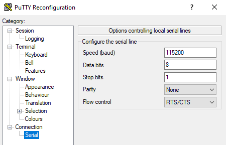
| + | ** 115,200 baud | ||
| + | ** RTS/CTS flow control | ||
| + | |||
| + | [[FILE:RPI_SPI8-puTTY_setup.PNG]] | ||
| + | |||
| + | * Hit ENTER to see menu | ||
| + | <pre> | ||
| + | Land Boards, LLC - RPi Card Test Station | ||
| + | 1 - Select RPP-UIO-16 Card | ||
| + | 2 - Select RPPSOC Card | ||
| + | 3 - Select RASPI-PLUS-GVS-CFG Card | ||
| + | 4 - Select RASPI-GVS Card | ||
| + | 5 - Select RASPI-PLUS-GVS Card | ||
| + | 6 - Select RPI-I2C-HUB Card | ||
| + | 7 - Select RPI-SPI8 Card | ||
| + | 8 - Select SPI-POTX2 Card (via RPI-SPI8) | ||
| + | R - Read EEPROM | ||
| + | W - Write EEPROM | ||
| + | B - Bounce LED across Card GPIOs | ||
| + | T - Test Card | ||
| + | D - Debug Card | ||
| + | ? - Print this menu | ||
| + | </pre> | ||
| + | * Select SPI-POTX2 Card by entering 8[ENTER] | ||
| + | <pre> | ||
| + | 8 | ||
| + | Selected SPI-POTX2 card (vis RPI-SPI8) | ||
| + | </pre> | ||
| + | |||
| + | === Create Sawtooth Output === | ||
| + | |||
| + | * Enter T[ENTER] - Create ramped output | ||
| + | <pre> | ||
| + | Testing SPI-POTX2 card (via RPI-SPI8), please wait | ||
| + | test_SPI_POTX2() - Reached function | ||
| + | test_SPI_POTX2() - Start SPI | ||
| + | test_SPI_POTX2() - Started SPI</pre> | ||
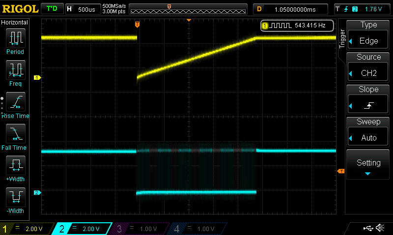
| + | * Use scope to observe ramped output on POT0 | ||
| + | ** CH 1 Yellow = SPI_CE0 | ||
| + | ** CH 2 Cyan = POT0 wiper | ||
| + | |||
| + | [[file:SPI-POTX2-14.png]] | ||
| + | |||
| + | === Test Software === | ||
| + | |||
| + | * Runs on [[RPI_PSOC5]] | ||
| + | * [https://github.com/land-boards/RasPi/tree/master/RPI_PSOC5/RPI_PSOC5_RPI_SPI8_CARD_TEST.cydsn GitHub repo] | ||
| + | ** [https://github.com/land-boards/RasPi/blob/master/RPI_PSOC5/RPI_PSOC5_CARD_TEST_STATION.cydsn/Test_RPI_SPI8.c Test_RPI_SPI8.c] - Bounce LED across [[LED-TEST-2]] card | ||
| + | |||
| + | * Runs on [[RPI_PSOC5]] | ||
| + | * Uses [[RPI_SPI8]] | ||
| + | * [https://github.com/land-boards/RasPi/tree/master/RPI_PSOC5/RPI_PSOC5_RPI_SPI8_CARD_TEST.cydsn GitHub repo] | ||
| + | ** [https://github.com/land-boards/RasPi/blob/master/RPI_PSOC5/RPI_PSOC5_RPI_SPI8_CARD_TEST.cydsn/Test_RPI_SPI8.c Test_RPI_SPI8.c] - Test with SPI-POTX2 card | ||
| + | |||
| + | == Changes == | ||
| + | |||
| + | === Rev 2 === | ||
| + | |||
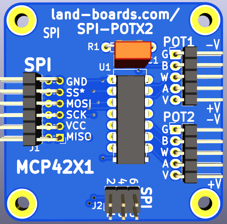
| + | * Swapped POT1 A, B pins to match POT0 and silkscreen | ||
| + | * Combined SPI connectors from 2 to 1 of 2x6 connector | ||
| + | * Added SPI pin names to reverse side silkscreen | ||
| + | |||
| + | [[file:SPI-POT_Rev2_FRONT__3D.png]] | ||
| + | |||
| + | === Rev X1 === | ||
| + | |||
| + | * POT1 A, B pins swapped on silkscreen | ||
| + | ** POT1 Vcc, GND taps can not be shunted directly - need jumper cables to correct | ||
== Assembly Sheet == | == Assembly Sheet == | ||
| − | * [[SPI-POTX2 Assembly Sheet]] | + | * [[SPI-POTX2 Rev 2 Assembly Sheet]] |
| + | * [[SPI-POTX2 Assembly Sheet|SPI-POTX2 Rev X1 Assembly Sheet]] | ||
Latest revision as of 15:27, 16 May 2022
Contents
Features
- Dual Digital potentiometer
- MCP4231 Dual Digital Pot
- 7-bit: 128 Resistors (129 Steps)
- Zero Scale to Full Scale Wiper operation
- 10K
- Other resistances optional: 5K, 50K, 100K
- Power on reset to half wiper value
- SPI Interface
- SPI Serial Interface (10 MHz, modes 0,0 & 1,1)
- High-Speed Read/Writes to wiper register
- 10 MHz (max SPI speed)
- 2.7V to 5.5V
- Daisy-chain SPI connector
- Slave Select (SS) should be star connected
- 49x49mm form factor
- (4) #4-40 mounting holes
Connectors
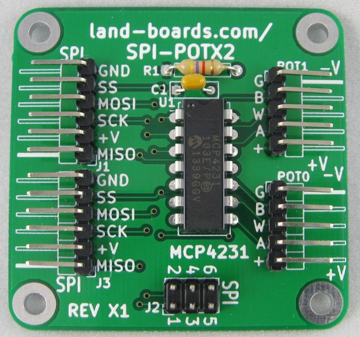
J1, J3 - SPI connector - Rev X1
- Two separate 1x5 headers
- Used for chaining to other cards
- MISO
- +V
- SCK
- MOSI
- SS
- GND
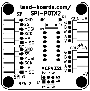
J1, J3 - SPI connector - Rev 2
- Single 2x6 right angle header
- Used for chaining to other cards
- MISO
- +V
- SCK
- MOSI
- SS
- GND
J2 - SPI Connector
- Matches Arduino SPI connector pinout
- MISO
- +V
- SCK
- MOSI
- SS
- GND
POT0
- GND
- B SIDE
- WIPER
- A SIDE
- +V
POT1 - Rev X1
- GND
- A SIDE
- WIPER
- B SIDE
- +V
- Rev X1 board has POT1 A, B Sides reversed on Silkscreen
- Impacts POT1 Vcc/GND jumpers
POT1 - Rev 2
- GND
- B SIDE
- WIPER
- A SIDE
- +V
- Rev 2 board updated so POT1 matches POT0
Driver Software
- Set channel number on GPIO_22 (A0), GPIO_27 (A1), GPIO_17 (A2)
- Do SPI transfer as 2 of 8-bit or 1 of 16-bit transfer(s)
Arduino Driver / Example Code
- SPI-POT-X2 GitHub Arduino Example Code
- Creates triangle wave output on both outputs
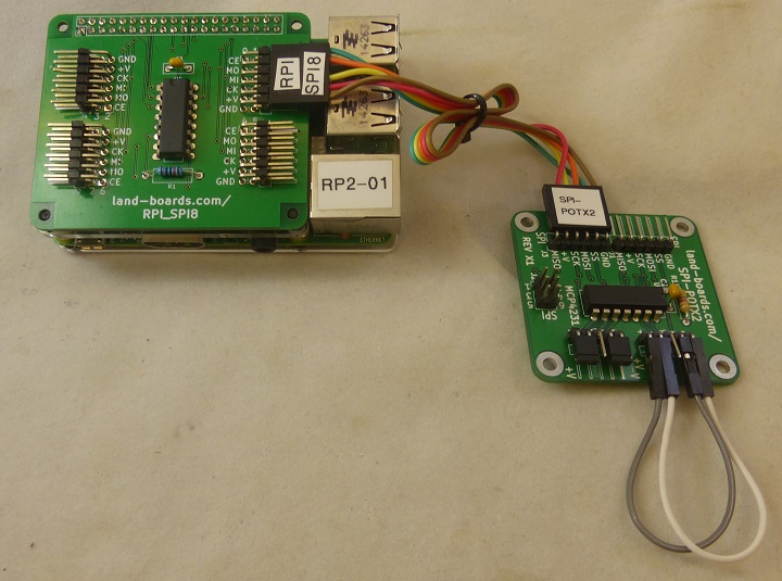
Raspberry Pi Example Code
- Test SPI-POTX2 Dual pot card on the Raspberry Pi using RPI_SPI8 SPI mux card
- Mux card is easy to include/exclude option in the code
# Set the next line to False if directly connecting to Raspberry Pi SPI bus
USING_RPI_SPI8_CARD = True
- Makes triangle waves on the pot wiper pins
- MCP4231_SPI_Test.py - Our GitHub repo
Raspberry Pi Reference Docs
Factory Test Procedure
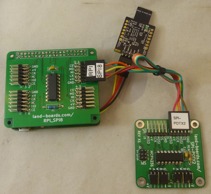
- Test SPI-POTX2 card on RPI_PSOC5 Test Station
Hardware Setup
SPI Cable
| RPI_SPI8 (Marking) | RPI_SPI8 Pin | SPI-POTX2 Pin | SPI-POTX2 Marking |
|---|---|---|---|
| Chip En (CE) | 1 | 5 | SS |
| MOSI (MO) | 2 | 4 | MOSI |
| MISO (MI) | 3 | 1 | MISO |
| SPICK (CK) | 4 | 3 | SCK |
| Vcc (+V) | 5 | 2 | +V |
| GND | 6 | 6 | GND |
Run Tests
- Run puTTY
- Find COM Port in Device Manager
- 115,200 baud
- RTS/CTS flow control
- Hit ENTER to see menu
Land Boards, LLC - RPi Card Test Station
1 - Select RPP-UIO-16 Card
2 - Select RPPSOC Card
3 - Select RASPI-PLUS-GVS-CFG Card
4 - Select RASPI-GVS Card
5 - Select RASPI-PLUS-GVS Card
6 - Select RPI-I2C-HUB Card
7 - Select RPI-SPI8 Card
8 - Select SPI-POTX2 Card (via RPI-SPI8)
R - Read EEPROM
W - Write EEPROM
B - Bounce LED across Card GPIOs
T - Test Card
D - Debug Card
? - Print this menu
- Select SPI-POTX2 Card by entering 8[ENTER]
8
Selected SPI-POTX2 card (vis RPI-SPI8)
Create Sawtooth Output
- Enter T[ENTER] - Create ramped output
Testing SPI-POTX2 card (via RPI-SPI8), please wait
test_SPI_POTX2() - Reached function
test_SPI_POTX2() - Start SPI
test_SPI_POTX2() - Started SPI
- Use scope to observe ramped output on POT0
- CH 1 Yellow = SPI_CE0
- CH 2 Cyan = POT0 wiper
Test Software
- Runs on RPI_PSOC5
- GitHub repo
- Test_RPI_SPI8.c - Bounce LED across LED-TEST-2 card
- Runs on RPI_PSOC5
- Uses RPI_SPI8
- GitHub repo
- Test_RPI_SPI8.c - Test with SPI-POTX2 card
Changes
Rev 2
- Swapped POT1 A, B pins to match POT0 and silkscreen
- Combined SPI connectors from 2 to 1 of 2x6 connector
- Added SPI pin names to reverse side silkscreen
Rev X1
- POT1 A, B pins swapped on silkscreen
- POT1 Vcc, GND taps can not be shunted directly - need jumper cables to correct

