Difference between revisions of "BASE-EP4CE6"
Jump to navigation
Jump to search
Blwikiadmin (talk | contribs) |
Blwikiadmin (talk | contribs) |
||
| (5 intermediate revisions by the same user not shown) | |||
| Line 76: | Line 76: | ||
[[File:P3-Connector.PNG]] | [[File:P3-Connector.PNG]] | ||
<pre> | <pre> | ||
| − | P3-Pin Port Pin P3-Pot | + | P3-Pin Port Pin P3-Port |
| + | 1 GND 2 NC | ||
| + | 3 55 4 58 | ||
| + | 5 53 6 54 | ||
| + | 7 51 8 52 | ||
| + | 9 49 10 50 | ||
| + | 11 44 12 46 | ||
| + | 13 42 14 43 | ||
| + | 15 38 16 39 | ||
| + | 17 33 18 34 | ||
| + | 19 31 20 32 | ||
| + | 21 28 22 30 | ||
| + | 23 GND 24 NC | ||
| + | 25 10 26 11 | ||
| + | 27 3 28 7 | ||
| + | 29 5 30 2 | ||
| + | 31 143 32 144 | ||
| + | 33 141 34 142 | ||
| + | 35 137 36 138 | ||
| + | 37 135 38 136 | ||
| + | 39 132 40 133 | ||
| + | 41 128 42 129 | ||
| + | 43 126 44 127 | ||
| + | </pre> | ||
| + | |||
| + | === P4 - Male pins === | ||
| + | |||
| + | * Flipped from the FPGA pinout | ||
| + | * Note that the physical pins on the schematic are reversed from the pinout on the card | ||
| + | |||
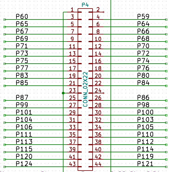
| + | [[File:P4-Connector.PNG]] | ||
| + | |||
| + | |||
| + | <pre> | ||
| + | P4-Pin Port Pin P4-Pot | ||
1 NC 2 GND | 1 NC 2 GND | ||
3 59 4 60 | 3 59 4 60 | ||
| Line 99: | Line 133: | ||
41 119 42 120 | 41 119 42 120 | ||
43 121 44 124 | 43 121 44 124 | ||
| − | |||
| − | |||
| − | |||
| − | |||
| − | |||
| − | |||
| − | |||
| − | |||
| − | |||
| − | |||
| − | |||
| − | |||
| − | |||
| − | |||
| − | |||
| − | |||
| − | |||
| − | |||
| − | |||
| − | |||
| − | |||
| − | |||
| − | |||
| − | |||
| − | |||
| − | |||
| − | |||
| − | |||
| − | |||
| − | |||
| − | |||
| − | |||
| − | |||
</pre> | </pre> | ||
| Line 142: | Line 143: | ||
* P9 = VCC | * P9 = VCC | ||
* P10 = GND | * P10 = GND | ||
| − | + | * Power/Grd pairs | |
** P6/P7 paired | ** P6/P7 paired | ||
** P5/P8 paired | ** P5/P8 paired | ||
| Line 168: | Line 169: | ||
* Map EP2 to EP4 card | * Map EP2 to EP4 card | ||
| − | ** Maps EP4 I/O connections to the EP2 card used for [[Multicomp_FPGA_Retrocomputer_Builds]] | + | ** Maps EP4 I/O connections to the EP2 card used for [[RetroComputers#Multicomp_FPGA_Retrocomputer_Builds|Multicomp]] |
== Rev X2 Checkout == | == Rev X2 Checkout == | ||
Latest revision as of 14:03, 25 January 2020
Contents
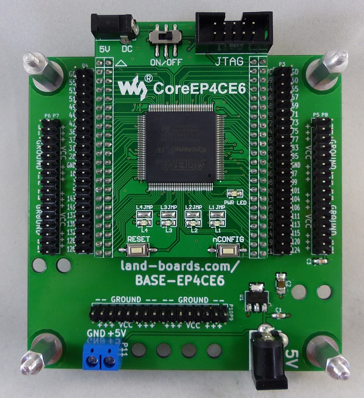
BASE-EP4CE6 Features
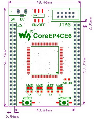
- WaveShare CoreEP4CE6 EP4CE6E22C8N FPGA Board
- Power LED
- (4) LEDs connected to I/O pins
- Config switch
- Reset switch
- Power Switch
- Power Switch does not turn board on/off when powered from this base board
- JTAG programming connnector
- Compatible with USB Blaster
- 5V power (or power through base board)
- Base board adds features
- Power Distribution
- GND/+3.3V on power strips
- All I/O pins brought out to header pins
- Allows easy connection for I/O cards
- Power Distribution
- Open Data Acquisition System compatible
- ODAS Form factor (95x95mm)
- 6-32 mounting holes in each corner
- Cable/zip ties hold down holes
Power domains
- 5V input through either the connectors on the base board or on the FPGA board
- Provides 5V to the CoreEP4CE6 board
- Only one source should be connected
- No protection if both are powered
- Only one source should be connected
- CoreEP4CE6 board creates 3.3V for its I/O pins
- 3.3V Power strips
- +3.3V Power Regulator on the base board powers the Power strips
- Use for powering external circuits
- Up to 1 Amp total
- 3.3V Power strips
Indicators
- LED1 - LED4
- LED1 - JP0 removes - connects to IO3
- LED2 - JP2 removes - connects to IO7
- LED3 - JP3 removes - connects to IO10
- LED4 - JP4 removes - connects to IO11
- LED Select jumpers (solder bridges)
Connectors
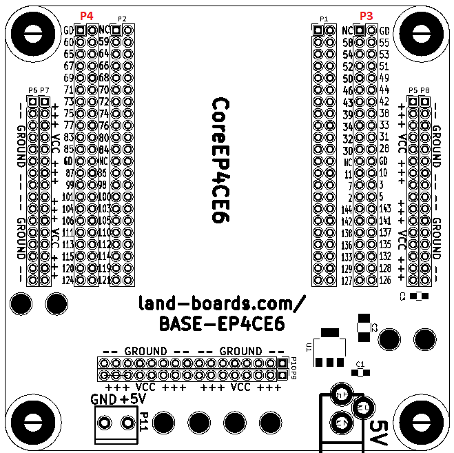
- P3 and P4 marking is different on the Rev X1 board
- These are the actual pin numbers
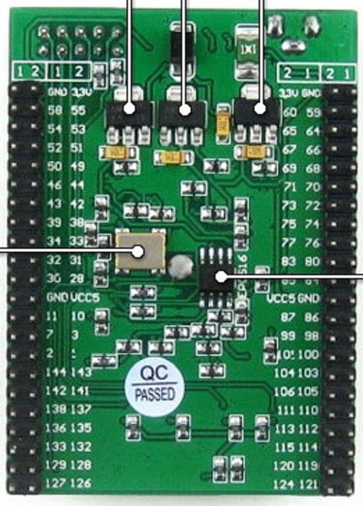
FPGA Board Pinout
- Pin numbers on the FPGA card are marked on the silkscreen on the bottom of the FPGA board
- Note that this is reflected when the card is installed onto the BASE board
- The base board also mirrors the adjacent pins
P1, P2 - FPGA Female connector
- Generally matches FPGA pinout
- Exceptions
- 3.3V from the FPGA card is not connected out of the FPGA card
- 3.3V power pins on the Base board are provided by the 3.3V regulator on the Base board
- 3.3V from the FPGA card is not connected out of the FPGA card
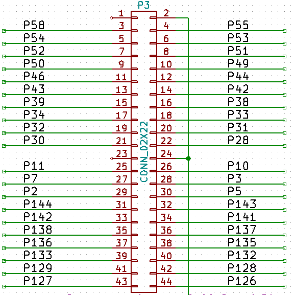
P3 - Male header pins
- Flipped from the FPGA pinout
- Note that the physical pins on the schematic are reversed from the pinout on the card
- Pin 1 from the FPGA is +3.3V
- Not connected on the header pins
- Base board is powered from the on-board 5V to 3.3V regulator
P3-Pin	Port	Pin	P3-Port
1	GND	2	NC
3	55	4	58
5	53	6	54
7	51	8	52
9	49	10	50
11	44	12	46
13	42	14	43
15	38	16	39
17	33	18	34
19	31	20	32
21	28	22	30
23	GND	24	NC
25	10	26	11
27	3	28	7
29	5	30	2
31	143	32	144
33	141	34	142
35	137	36	138
37	135	38	136
39	132	40	133
41	128	42	129
43	126	44	127
P4 - Male pins
- Flipped from the FPGA pinout
- Note that the physical pins on the schematic are reversed from the pinout on the card
P4-Pin	Port	Pin	P4-Pot
1	NC	2	GND
3	59	4	60
5	64	6	65
7	66	8	67
9	68	10	69
11	70	12	71
13	72	14	73
15	74	16	75
17	76	18	77
19	80	20	83
21	84	22	85
23	NC	24	GND
25	86	26	87
27	98	28	99
29	100	30	101
31	103	32	104
33	105	34	106
35	110	36	111
37	112	38	113
39	114	40	115
41	119	42	120
43	121	44	124
P5-P10 Power Connector
- P5 = VCC
- P6 = GND
- P7 = VCC
- P8 = GND
- P9 = VCC
- P10 = GND
- Power/Grd pairs
- P6/P7 paired
- P5/P8 paired
- P9/P10 paired
P11 - 5V Terminal Block
- 5mm, 2-pin
- 5V and GND
- Connects directly to the 5V barrel connector
- Only connect one source of input power to the Base board
5V Barrel Connector
- 5V input power to the card
- 5V and GND
- Connects directly to the 5V terminal block
- Only connect one source of input power to the Base board
FPGA Board Physical
Retro-Computer (MultiComp) Map EP2 to EP4 card
- Map EP2 to EP4 card
- Maps EP4 I/O connections to the EP2 card used for Multicomp
Rev X2 Checkout
- WIP
Rev X1 Checkout
- Connectors are swapped
- P3 and P4 Silkscreen is wrong
- Power is OK since the two connectors have the same pinouts for power
- Corrected silkscreen is as follows
