Difference between revisions of "ESP32-I2C-HUB"
Jump to navigation
Jump to search
Blwikiadmin (talk | contribs) |
Blwikiadmin (talk | contribs) |
||
| Line 154: | Line 154: | ||
=== Right GVS connector === | === Right GVS connector === | ||
| + | |||
| + | * Gnd/3.3V/Signal | ||
# P23/MOSI | # P23/MOSI | ||
Revision as of 16:08, 12 January 2020
Contents
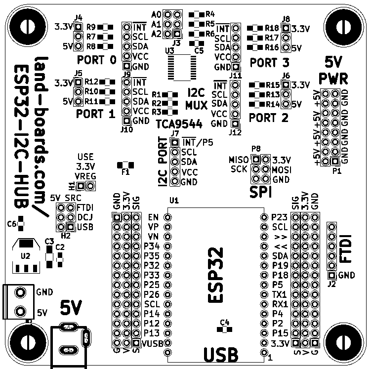
- 1 Feature
- 2 Schematic
- 3 Connectors
- 3.1 H1 - 3.3V from on-board regulator Header
- 3.2 H2 - 5V SRC Header
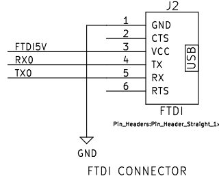
- 3.3 J2 - FTDI
- 3.4 J3 - I2C Mux Base Address Select Jumpers
- 3.5 J7 - I2C Interface
- 3.6 J4, J5, J6, J8 - I2C Power Select (Ports #0-#3)
- 3.7 J9, J10, J11, J12 - I2C interfaces #0-#3
- 3.8 P1 - 5V Power
- 3.9 P8 - SPIbus connector
- 3.10 Left GVS connector
- 3.11 Right GVS connector
- 4 Software Support
- 5 Assembly Sheet
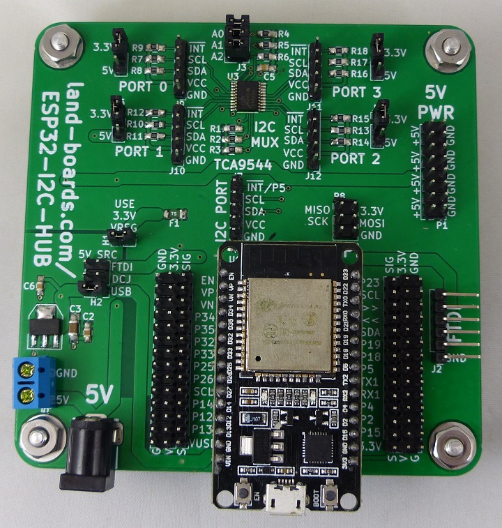
Feature
- ESP32 breakout board
- Requires specific version of ESP32 board
- GVS (Ground, Voltage, Signal) for all ESP32 pins
- 4-channel I2C Hub
- TCA9544 - 4-Channel I2C and SMBus Multiplexer With Interrupt Logic
- Isolated I2C channels
- Interrupt for each I2C channel
- I2C Channels can be independently powered with 3.3V or 5V
- Jumper selectable I2C base address
- GVS (Ground, Voltage, Signal) for all ESP32 pins
- FTDI header
- SPI bus header
- 5V power source selection/distribution
- 5V sources - USB, 5mm terminal block, DC jack
- On-board 3.3V power regulator (doesn't stress the ESP32 regulator)
- 95x95mm ODAS form factor
- 6-32 mounting holes
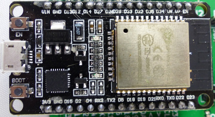
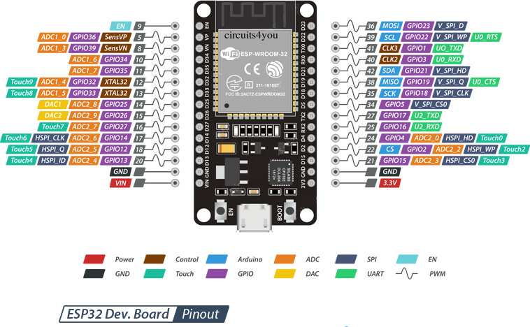
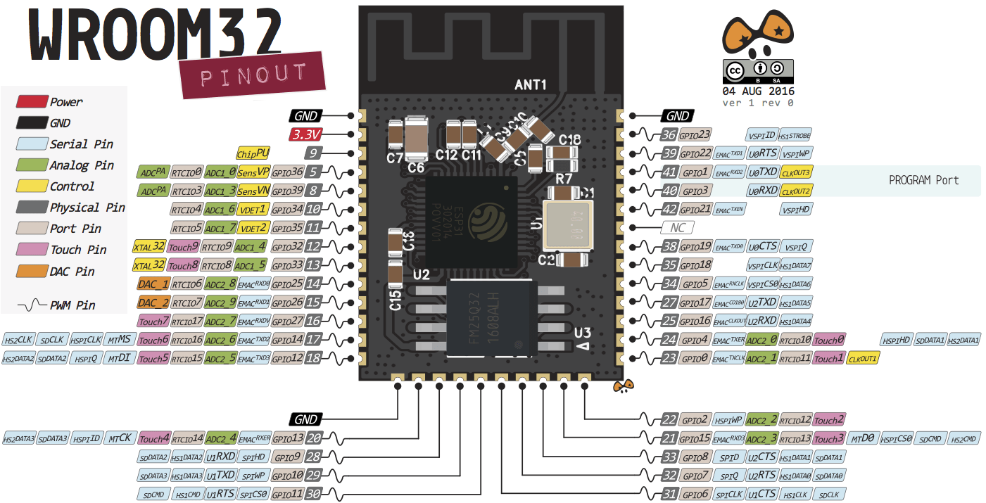
ESP-32 Module
- Board details
- On board Blue LED = Arduino Pin 2
Schematic
Connectors
H1 - 3.3V from on-board regulator Header
- Install jumper
- Alternate for 3.3V power is to install S to V jumper at 3.3V header position (bottom right)
- H1 should not be installed for that case
H2 - 5V SRC Header
- 2x3 header
- Care must be taken to install the correct jumpers
- USB jumper sends out 5V when a USB cable is connected to the ESP32 module
- USB jumper sends 5V into the ESP32 module when there is no USB cable connected to the ESP32 module
Power from USB on ESP32 module
- Do not install FTDI jumper
- Do not install DCJ jumper
- Install USB jumper
Power from 5V jack
- Do not install FTDI jumper
- Install DCJ jumper
- Install USB jumper
Power from FTDI
- Unstall FTDI jumper
- Do not install DCJ jumper
- Install USB jumper
J2 - FTDI
J3 - I2C Mux Base Address Select Jumpers
- A0-A2
- Install for 0
- Remove for 1
J7 - I2C Interface
- Also goes to the I2C Hub chip
- INT* (GPIO5)
- SCL
- SDA
- VCC
- GND
J4, J5, J6, J8 - I2C Power Select (Ports #0-#3)
- Selects 3.3V or 5V on I2C
- 1-2 = 3.3V
- 2-3 = 5V
J9, J10, J11, J12 - I2C interfaces #0-#3
- GND
- VCC
- SDA
- SCL
- INT*
P1 - 5V Power
- 2x8 pin header
P8 - SPIbus connector
- MISO
- 3.3V
- SCK
- MOSI
- n/c
- GND
Left GVS connector
- Gnd/3.3V/Signal
- EN (Pull low to shut off 3.3V reg)
- VP/P36
- VN/P39
- P34/P34
- P35/A7
- P32/A4
- P33/A5
- P25/A8
- P26/A9
- P27/SCL
- P14/SD_CLK
- P12/SD_D2
- P13/SD_D3
- VUSB
Right GVS connector
- Gnd/3.3V/Signal
- P23/MOSI
- SCL/RTS1
- P1/TX
- I3/RX
- P21/SDA
- P19/CTS0
- P18/SCK
- P5
- P17/TX2
- P16/RX2
- P4/SD_D1
- P2/SD_D0
- P15/SD_CMD
- 3.3V
