Difference between revisions of "LB-6802-01"
Jump to navigation
Jump to search
Blwikiadmin (talk | contribs) (→PLD) |
Blwikiadmin (talk | contribs) |
||
| Line 28: | Line 28: | ||
==== PLD Listing ==== | ==== PLD Listing ==== | ||
| + | |||
| + | <PRE> | ||
| + | Name LB-6802-01_PLD; | ||
| + | Partno ATF16V8B; | ||
| + | Date 08/24/24; | ||
| + | Revision 01; | ||
| + | Designer DOUG G; | ||
| + | Company LAND BOARDS LLC; | ||
| + | Assembly LB680201_U2; | ||
| + | Location Rustbelt, US; | ||
| + | Device G16V8; | ||
| + | |||
| + | /* | ||
| + | */ | ||
| + | |||
| + | |||
| + | /* Control inputs */ | ||
| + | PIN 1 = CLK; | ||
| + | PIN 2 = CPUA12; | ||
| + | PIN 3 = CPUA13; | ||
| + | PIN 4 = CPUA14; | ||
| + | PIN 5 = CPUA15; | ||
| + | PIN 6 = CPUREAD; | ||
| + | PIN 7 = VPB; /* Added as wire on Rev 1 PCB */ | ||
| + | PIN 8 = VPA; | ||
| + | PIN 9 = VDA; | ||
| + | |||
| + | /* Address Decode and Chip Select outputs */ | ||
| + | PIN 12 = !ROMCS; | ||
| + | PIN 13 = !IOCS; | ||
| + | PIN 14 = !MEMRD; | ||
| + | PIN 16 = !RAMCS; | ||
| + | PIN 18 = RDY; | ||
| + | |||
| + | ROMCS = CPUA15 & CPUA14 & VPB; | ||
| + | |||
| + | RAMCS = !CPUA15 & VPB /* 0x0000-0x7FFF 32KB SRAM */ | ||
| + | # CPUA15 & !CPUA14 & !CPUA13 & VPB; /* 0x8000-0x9FFF Free (8KB */ | ||
| + | |||
| + | IOCS = CPUA15 & !CPUA14 & CPUA13 & VPB; /* 0xA000-0xBFFF Serial (ACIA) */ | ||
| + | |||
| + | RDY = VPB; | ||
| + | |||
| + | MEMRD = CPUREAD & VPB; | ||
| + | </PRE> | ||
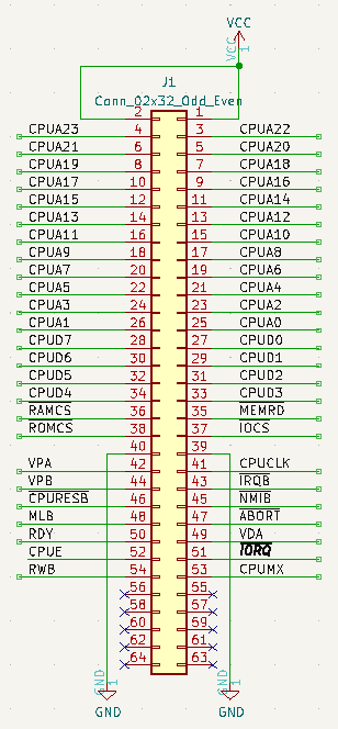
=== Backplane Connector === | === Backplane Connector === | ||
Revision as of 15:25, 24 August 2024
Contents
Features
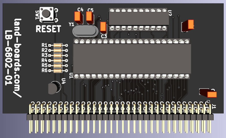
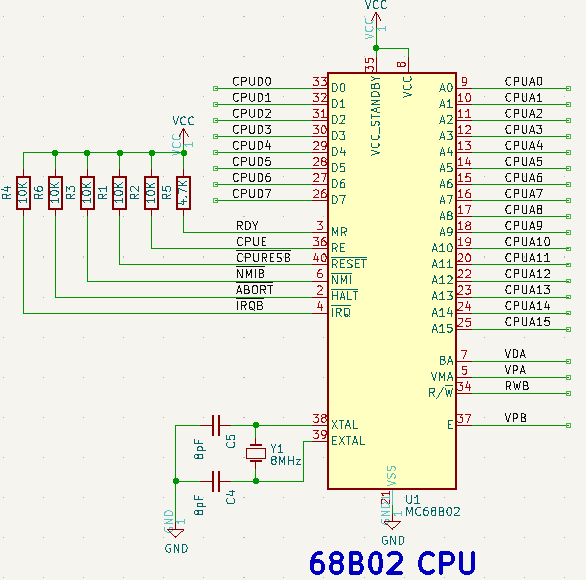
- 68B02 CPU
- 1.8432 MHz clock
- MC6802 is fully compatible with MC6800 but without messy two-phase clocking
Memory Map
- 0x0000-0x7FFF 32KB SRAM
- 0x8000-0xBFFF Serial (68B50 ACIA)
- 0xC000-0xFFFF 16KB EPROM
Design
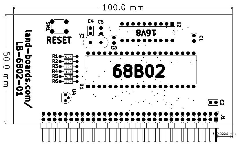
CPU
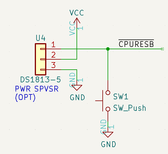
Power Supervisor/Reset
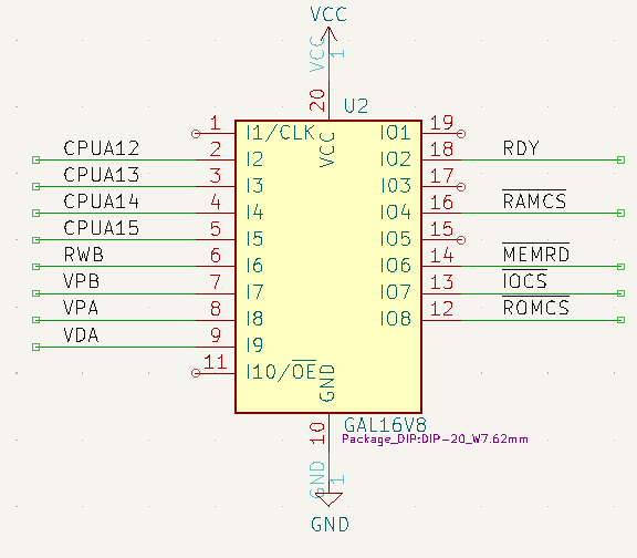
PLD
PLD Listing
Name       LB-6802-01_PLD;
Partno     ATF16V8B;
Date       08/24/24;
Revision   01;
Designer   DOUG G;
Company    LAND BOARDS LLC;
Assembly   LB680201_U2;
Location   Rustbelt, US;
Device     G16V8;

/*
*/


/* Control inputs */
PIN    1   = CLK;
PIN    2   = CPUA12;
PIN    3   = CPUA13;
PIN    4   = CPUA14;
PIN    5   = CPUA15;
PIN    6   = CPUREAD;
PIN    7   = VPB;		/* Added as wire on Rev 1 PCB	*/
PIN    8   = VPA;
PIN    9   = VDA;

/* Address Decode and Chip Select outputs */
PIN    12  = !ROMCS;
PIN    13  = !IOCS;
PIN    14  = !MEMRD;
PIN    16  = !RAMCS;
PIN    18  = RDY;

ROMCS = CPUA15 & CPUA14 & VPB;

RAMCS = !CPUA15 & VPB						/* 0x0000-0x7FFF 32KB SRAM */
#        CPUA15 & !CPUA14 & !CPUA13 & VPB;	/* 0x8000-0x9FFF Free (8KB	*/

IOCS = CPUA15 & !CPUA14 & CPUA13 & VPB;		/* 0xA000-0xBFFF Serial (ACIA)	*/

RDY = VPB;

MEMRD = CPUREAD & VPB;
