Difference between revisions of "LB-Z80-01"
Jump to navigation
Jump to search
Blwikiadmin (talk | contribs) |
Blwikiadmin (talk | contribs) |
||
| Line 28: | Line 28: | ||
* Oscillator 8 MHz nominal on card | * Oscillator 8 MHz nominal on card | ||
* Reset switch/power monitor | * Reset switch/power monitor | ||
| + | |||
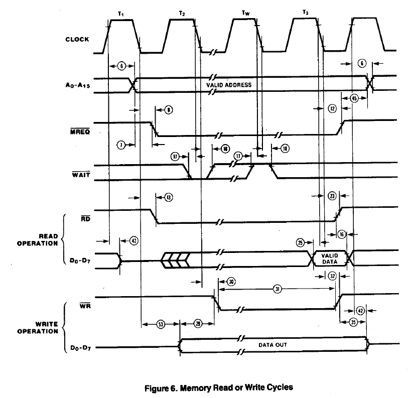
| + | === Memory Access Timing === | ||
| + | |||
| + | [[File:Z80_Mem_Rd_Wr.PNG]] | ||
=== Oscillator === | === Oscillator === | ||
Revision as of 23:04, 18 September 2024
Contents
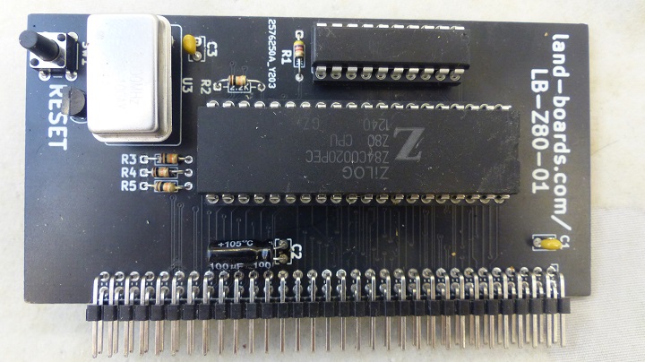
Features
- Z80 CPU
- Oscillator 8 MHz nominal on card
- Reset switch/power monitor
- Address decoder PLD drives RAM/ROM/IO chip selects
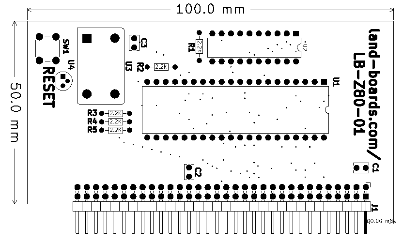
- 100x50mm card
Memory Map
- 0x0000-0x1FFF 8KB ROM
- 0x2000-0xFFFF 56KB SRAM
- I/O
- 0x00-0x7F - Free
- 0x80-0x81 - Serial port (ACIA)
Design
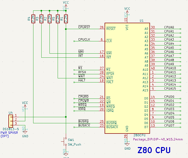
CPU and Power Supervisor/Reset
- Z80 CPU
- Oscillator 8 MHz nominal on card
- Reset switch/power monitor
Memory Access Timing
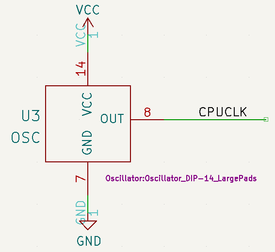
Oscillator
- 8MHZ or 10 MHz oscillator
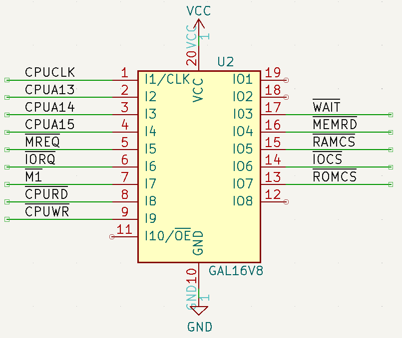
PLD
- ATF16V8B part
- TL866ii Plus Programmer
PLD Listing
Name       LB-Z80-01_PLD;
Partno     ATF16V8B;
Date       09/17/20;
Revision   01;
Designer   DOUG G;
Company    LAND BOARDS LLC;
Assembly   LB-Z80-01_U2;
Location   Rustbelt, US;
Device     G16V8;

/*
*/


/* Control inputs */
PIN    1   = CLK;
PIN    2   = CPUA13;
PIN    3   = CPUA14;
PIN    4   = CPUA15;
PIN    5   = !MREQ;
PIN    6   = !IORQ;
PIN    7   = !M1;
PIN    8   = !CPURD;
PIN    9   = !CPUWR;

/* Address Decode and Chip Select outputs */
PIN    13  = !ROMCS;
PIN    14  = !IOCS;
PIN    16  = !MEMRD;
PIN    15  = !RAMCS;
PIN    18  = !WAIT;

ROMCS = !CPUA15 & !CPUA14 & !CPUA13 & MREQ & CPURD;

RAMCS = CPUA15 & MREQ
#       CPUA14 & MREQ
#       CPUA13 & MREQ;

IOCS = !M1 & IORQ;

WAIT = !MREQ # !IORQ;

MEMRD = CPURD;
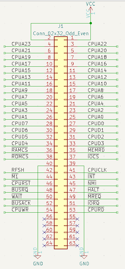
Backplane Connector
Software
Mechanicals
Checkout
Rev 1
- Didn't use silkscreen values, used
- R1 = 4.7K
- Other resistors are 10K
- Z80 nop tester nop = 0x00
- Refresh complicates this
