Difference between revisions of "PDP-8 Front Panel"
Jump to navigation
Jump to search
Blwikiadmin (talk | contribs) |
Blwikiadmin (talk | contribs) |
||
| Line 30: | Line 30: | ||
* 50 pin connector matches [[RETRO-EP4CE15]] Card | * 50 pin connector matches [[RETRO-EP4CE15]] Card | ||
| − | ** Extra pins | + | ** Extra power and ground pins |
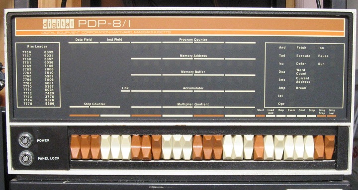
== Real PDP-8/I Front Panel == | == Real PDP-8/I Front Panel == | ||
[[File:PDP-8i_FrontPanel_720px.jpg]] | [[File:PDP-8i_FrontPanel_720px.jpg]] | ||
Revision as of 13:31, 18 April 2021
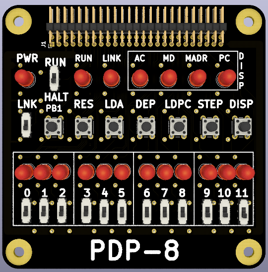
Features
- 12 LEDs
- Display options: PC, Memory Address, Memory Data, Accumulator
- Value Slide Switches
- Enter values: PC, Memory Address, Memory Data, Accumulator
- Display select pushbutton
- Cycles between PC, Memory Address, Memory Data, Accumulator
- Pushbutton Switches
- STEP pushbutton
- LDPC pushbutton - Load PC from Value Slide Switches
- DEP pushbutton - Store value from Value Slide Switches to memory
- LDA pushbutton - Store value from Value Slide Switches to Accumulator
- RES - Reset pushbutton - resets CPU
- PB1 - spare
- LNK - Link value slide switch
- DISP LEDs
- PC - 12 LEDs display Program Counter value
- PC - 12 LEDs display Memory Address value
- PC - 12 LEDs display Memory Data value
- PC - 12 LEDs display Accumulator value
- LINK LED - Displays Link value
- FN1 spare LED
- RUN/HALT slide switch
- PWR - Power LED
PDP-8 FPGA Design
- 50 pin connector matches RETRO-EP4CE15 Card
- Extra power and ground pins

