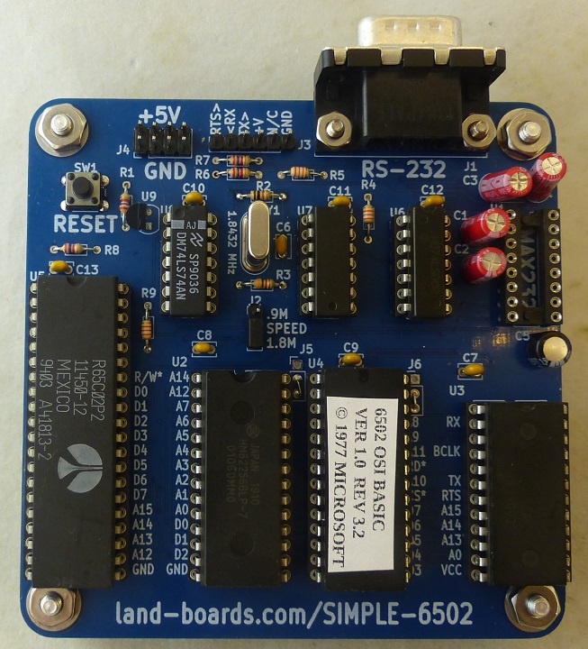
Difference between revisions of "SIMPLE-6502"
Jump to navigation
Jump to search
Blwikiadmin (talk | contribs) |
Blwikiadmin (talk | contribs) |
||
| (142 intermediate revisions by the same user not shown) | |||
| Line 1: | Line 1: | ||
| − | [[FILE: | + | [[File:tindie-mediums.png|link=https://www.tindie.com/products/34959/]] |
| + | |||
| + | [[FILE:SIMPLE-6502_P1090254-720pxV.jpg]] | ||
| + | |||
| + | <video type="youtube">p5mwMwwM-R0</video> | ||
== Features == | == Features == | ||
| Line 5: | Line 9: | ||
* Build of [http://searle.x10host.com/6502/Simple6502.html Grant Searles's Simple 6502 CPU] | * Build of [http://searle.x10host.com/6502/Simple6502.html Grant Searles's Simple 6502 CPU] | ||
** Runs Microsoft (OSI) BASIC | ** Runs Microsoft (OSI) BASIC | ||
| − | * 6502 CPU | + | * [https://github.com/land-boards/lb-boards/blob/master/RetroCPUs/SIMPLE-6502/PARTS/R65C02P3_Datasheet.pdf 65C02 CPU] |
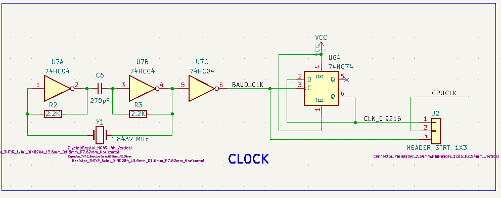
| − | * 0.9216 or 1.8432 MHz clock | + | * 0.9216 or 1.8432 MHz clock - jumper selectable |
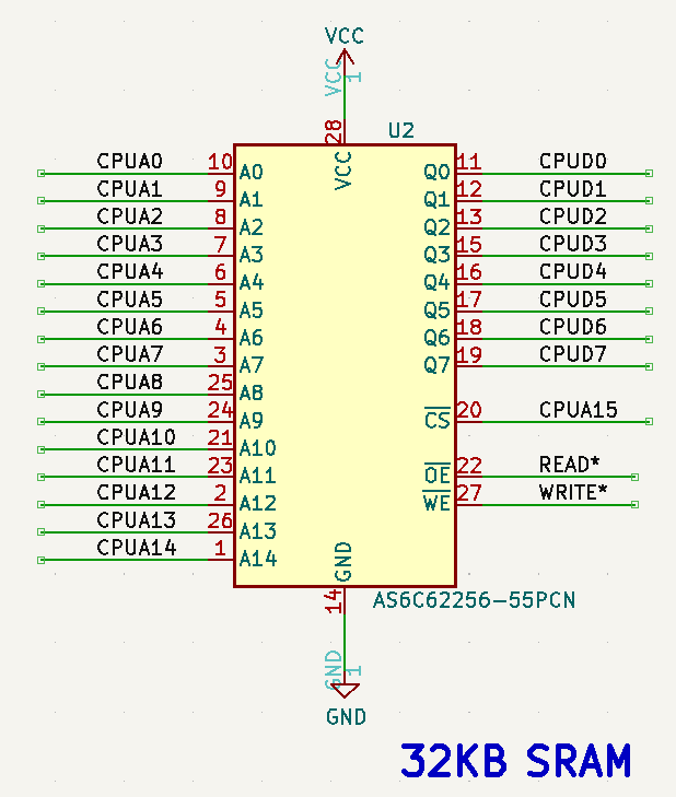
| − | * 32KB SRAM | + | * [https://github.com/land-boards/lb-boards/blob/master/RetroCPUs/SIMPLE-6502/PARTS/AS6C62256_23_March_2016_rev1_2-1288423.pdf 32KB SRAM] |
* 16KB EPROM/EEPROM | * 16KB EPROM/EEPROM | ||
| − | * 68B50 Serial Port (ACIA) | + | ** Using 1/2 of [https://github.com/land-boards/lb-boards/blob/master/RetroCPUs/SIMPLE-6502/PARTS/SST27SF256.pdf SST27SF256] - 32KB Flash Memory |
| − | ** RS-232 port | + | * [https://github.com/land-boards/lb-boards/blob/master/RetroCPUs/SIMPLE-6502/PARTS/MC68B50_43633.pdf 68B50 Serial Port (ACIA)] |
| + | ** [https://github.com/land-boards/lb-boards/blob/master/RetroCPUs/SIMPLE-6502/PARTS/max232.pdf MAX232] RS-232 port or | ||
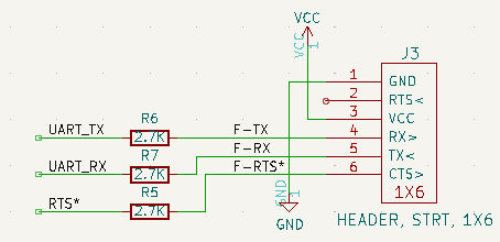
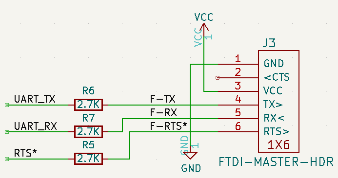
** Header for FTDI | ** Header for FTDI | ||
** 115,200 baud | ** 115,200 baud | ||
| − | * Reset switch with optional Power Supervisor | + | * Reset switch with optional [https://github.com/land-boards/lb-boards/blob/master/RetroCPUs/SIMPLE-6502/PARTS/ds1813-maxim%20integrated%20products_1178753.pdf DS1813 5V Power Supervisor] |
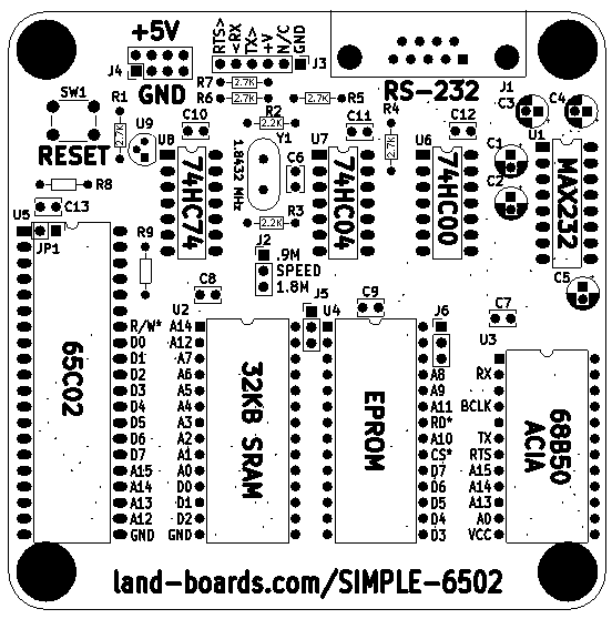
* 95x95mm card | * 95x95mm card | ||
* (4) 6-32 mounting holes | * (4) 6-32 mounting holes | ||
| Line 22: | Line 27: | ||
* 0x8000-0x9FFF Free Space (8KB) | * 0x8000-0x9FFF Free Space (8KB) | ||
* 0xA000-0xBFFF Serial (ACIA) | * 0xA000-0xBFFF Serial (ACIA) | ||
| − | * 0xC000- | + | * 0xC000-0xFFFF 16KB EPROM |
=== Chip Set === | === Chip Set === | ||
| Line 30: | Line 35: | ||
[[file:LB_65C02_PARTS.jpg]] | [[file:LB_65C02_PARTS.jpg]] | ||
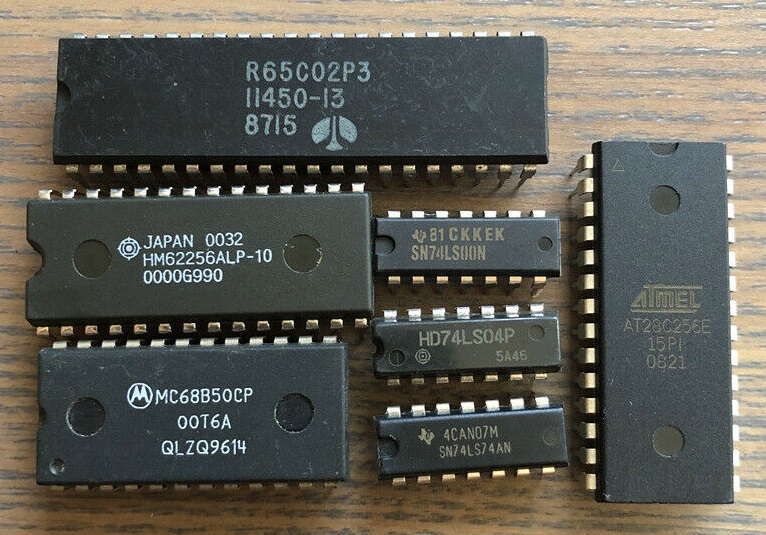
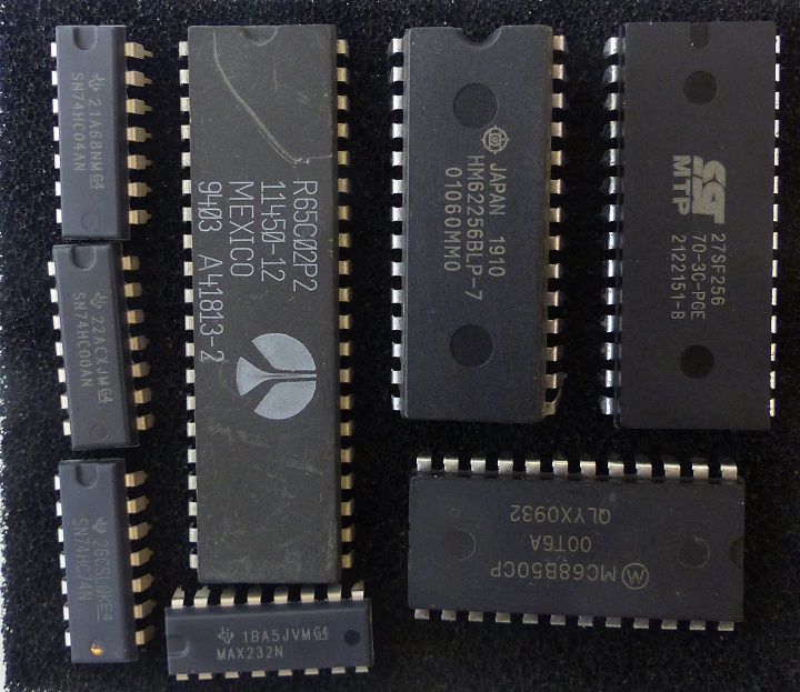
| − | * | + | * Picture shows 3 MHz CPU |
| + | * Received 2 MHz CPU | ||
| + | * As received: | ||
[[file:SIMPLE-6502_P1090155-720px.jpg]] | [[file:SIMPLE-6502_P1090155-720px.jpg]] | ||
| Line 46: | Line 53: | ||
== Design == | == Design == | ||
| − | + | === CPU === | |
[[file:U5_CPU_6502.PNG]] | [[file:U5_CPU_6502.PNG]] | ||
| − | * EPROM/EPROM | + | ==== R6502 CPU Timing ==== |
| + | |||
| + | [[file:R6502_Timing-01.PNG]] | ||
| + | [[file:R6502_Timing-02.PNG]] | ||
| + | |||
| + | ==== R65C02 vs W65C02 vs W65C816 CPUs ==== | ||
| + | |||
| + | {| class="wikitable" | ||
| + | ! U5 Pin | ||
| + | ! U5 Pin Name | ||
| + | ! Sig Name | ||
| + | ! Pullup | ||
| + | ! R65C02 sig | ||
| + | ! W65C02 sig | ||
| + | ! W65C816 sig | ||
| + | |- | ||
| + | | 1 | ||
| + | | VSS/VPB | ||
| + | | JP1 GNDs | ||
| + | | N | ||
| + | | VSS (IN) | ||
| + | | VPB (OUT) | ||
| + | | VPB (OUT) | ||
| + | |- | ||
| + | | 3 | ||
| + | | PH1OUT/ABORT | ||
| + | | NC | ||
| + | | N | ||
| + | | PH1OUT (OUT) | ||
| + | | PH1OUT (OUT) | ||
| + | | ABORT (IN) | ||
| + | |- | ||
| + | | 5 | ||
| + | | NC/MLB | ||
| + | | NC | ||
| + | | N | ||
| + | | NC | ||
| + | | MLB (OUT) | ||
| + | | MLB (OUT) | ||
| + | |- | ||
| + | | 7 | ||
| + | | SYNC/VPA | ||
| + | | NC | ||
| + | | N | ||
| + | | SYNC (OUT) | ||
| + | | SYNC (OUT) | ||
| + | | VPA (OUT) | ||
| + | |- | ||
| + | | 35 | ||
| + | | NC/E | ||
| + | | NC | ||
| + | | N | ||
| + | | NC | ||
| + | | NC | ||
| + | | EM/NAT (OUT) | ||
| + | |- | ||
| + | | 36 | ||
| + | | NC/BE | ||
| + | | Pull up | ||
| + | | Y | ||
| + | | NC | ||
| + | | BE (IN) | ||
| + | | BE (IN) | ||
| + | |- | ||
| + | | 37 | ||
| + | | PH0IN/PH2IN | ||
| + | | CPUCLK | ||
| + | | N | ||
| + | | PH0IN | ||
| + | | PH2IN | ||
| + | | PH2IN | ||
| + | |- | ||
| + | | 38 | ||
| + | | SO/MX | ||
| + | | VCC | ||
| + | | VCC | ||
| + | | SO* (IN) | ||
| + | | SOB (IN) | ||
| + | | MX (OUT) | ||
| + | |- | ||
| + | | 39 | ||
| + | | PH2OUT/VDA | ||
| + | | PH2_OUT | ||
| + | | N | ||
| + | | PH2OUT (OUT) | ||
| + | | PH2OUT (OUT) | ||
| + | | VDA(OUT) | ||
| + | |- | ||
| + | |} | ||
| + | |||
| + | * Need to lift U5-38 to use W65C816 CPU | ||
| + | |||
| + | [[file:R65C02_vs_W65C02_w65c816_Pinout_800PX.png]] | ||
| + | |||
| + | ===== VDA/VPA (65C816) ===== | ||
| + | |||
| + | * VDA/VPA | ||
| + | ** 00, Internal operation (invalid address bus) | ||
| + | ** 01, Valid Program Address | ||
| + | ** 10, Valid Data Address | ||
| + | ** 11, Opcode-fetch | ||
| + | |||
| + | === EPROM/EPROM === | ||
| + | |||
| + | * [[TL866ii Plus Programmer]] | ||
[[file:U4_EEPROM.PNG]] | [[file:U4_EEPROM.PNG]] | ||
| − | + | === SRAM === | |
[[file:U2_SRAM.PNG]] | [[file:U2_SRAM.PNG]] | ||
| − | + | === Clock (Rev 1) === | |
[[file:U7_U8_CLOCK.PNG]] | [[file:U7_U8_CLOCK.PNG]] | ||
| − | * | + | === Clock (Rev 2) === |
| + | |||
| + | [[file:U7_U8_CLOCK_v2.PNG]] | ||
| + | |||
| + | === UART === | ||
| + | |||
| + | * Can only use RS-232 or FTDI - one at a time | ||
| + | ** Put MAX232 in a socket if you want flexibility | ||
| + | ** Remove MAX232 if you want to use FTDI | ||
[[file:U1_U3_UART.PNG]] | [[file:U1_U3_UART.PNG]] | ||
| − | * FTDI | + | === FTDI === |
| + | |||
| + | * Does not match Grant's pinout | ||
| + | * Can only use RS-232 or FTDI - one at a time | ||
[[file:J3_FTDI.PNG]] | [[file:J3_FTDI.PNG]] | ||
| Line 77: | Line 199: | ||
* DB-9 Male | * DB-9 Male | ||
| + | * Matches Grant's pinout | ||
* Pinout | * Pinout | ||
| Line 95: | Line 218: | ||
=== J3 - FTDI / TTL Serial === | === J3 - FTDI / TTL Serial === | ||
| + | |||
| + | * Requires a FTDI cross-over cable | ||
| + | |||
| + | [[FILE:SIMPLE-6502_J3_FTDI.PNG]] | ||
# GND | # GND | ||
| Line 112: | Line 239: | ||
[[FILE:SIMPLE-6502_J5_J6.PNG]] | [[FILE:SIMPLE-6502_J5_J6.PNG]] | ||
| + | |||
| + | * J5 - EPROM Pin 1 jumper | ||
| + | ** 1-2 for 28C64, 28C256 (Pull WE to VCC) | ||
| + | ** 2-3 for 27256, 27SF256, 27512 (Pull A14 to GND) | ||
| + | * J6 - EPROM Pin 27 jumper | ||
| + | ** GND (2-3) | ||
| + | |||
| + | ==== EEPROM Pin Table ==== | ||
{| class="wikitable" | {| class="wikitable" | ||
! 27512 | ! 27512 | ||
! 27256 | ! 27256 | ||
| + | ! 27SF256 | ||
! 28C256 | ! 28C256 | ||
! 27128 | ! 27128 | ||
| Line 127: | Line 263: | ||
! 27128 | ! 27128 | ||
! 28C256 | ! 28C256 | ||
| + | ! 27SF256 | ||
! 27256 | ! 27256 | ||
! 27512 | ! 27512 | ||
|- | |- | ||
| A15 | | A15 | ||
| + | | VPP | ||
| VPP | | VPP | ||
| A14 | | A14 | ||
| Line 139: | Line 277: | ||
| | | | ||
| 28 | | 28 | ||
| + | | VCC | ||
| VCC | | VCC | ||
| VCC | | VCC | ||
| Line 146: | Line 285: | ||
| VCC | | VCC | ||
|- | |- | ||
| + | | A12 | ||
| A12 | | A12 | ||
| A12 | | A12 | ||
| Line 159: | Line 299: | ||
| PGM | | PGM | ||
| WE* | | WE* | ||
| + | | A14 | ||
| A14 | | A14 | ||
| A14 | | A14 | ||
|- | |- | ||
| + | | A7 | ||
| A7 | | A7 | ||
| A7 | | A7 | ||
| Line 173: | Line 315: | ||
| A13 | | A13 | ||
| N/C | | N/C | ||
| + | | A13 | ||
| A13 | | A13 | ||
| A13 | | A13 | ||
| Line 178: | Line 321: | ||
| A13 | | A13 | ||
|- | |- | ||
| + | | A6 | ||
| A6 | | A6 | ||
| A6 | | A6 | ||
| Line 187: | Line 331: | ||
| | | | ||
| 25 | | 25 | ||
| + | | A8 | ||
| A8 | | A8 | ||
| A8 | | A8 | ||
| Line 194: | Line 339: | ||
| A8 | | A8 | ||
|- | |- | ||
| + | | A5 | ||
| A5 | | A5 | ||
| A5 | | A5 | ||
| Line 203: | Line 349: | ||
| | | | ||
| 24 | | 24 | ||
| + | | A9 | ||
| A9 | | A9 | ||
| A9 | | A9 | ||
| Line 210: | Line 357: | ||
| A9 | | A9 | ||
|- | |- | ||
| + | | A4 | ||
| A4 | | A4 | ||
| A4 | | A4 | ||
| Line 219: | Line 367: | ||
| | | | ||
| 23 | | 23 | ||
| + | | A11 | ||
| A11 | | A11 | ||
| A11 | | A11 | ||
| Line 226: | Line 375: | ||
| A11 | | A11 | ||
|- | |- | ||
| + | | A3 | ||
| A3 | | A3 | ||
| A3 | | A3 | ||
| Line 235: | Line 385: | ||
| | | | ||
| 22 | | 22 | ||
| + | | OE* | ||
| OE* | | OE* | ||
| OE* | | OE* | ||
| Line 242: | Line 393: | ||
| OE* | | OE* | ||
|- | |- | ||
| + | | A2 | ||
| A2 | | A2 | ||
| A2 | | A2 | ||
| Line 251: | Line 403: | ||
| | | | ||
| 21 | | 21 | ||
| + | | A10 | ||
| A10 | | A10 | ||
| A10 | | A10 | ||
| Line 258: | Line 411: | ||
| A10 | | A10 | ||
|- | |- | ||
| + | | A1 | ||
| A1 | | A1 | ||
| A1 | | A1 | ||
| Line 267: | Line 421: | ||
| | | | ||
| 20 | | 20 | ||
| + | | CE* | ||
| CE* | | CE* | ||
| CE* | | CE* | ||
| Line 274: | Line 429: | ||
| CE* | | CE* | ||
|- | |- | ||
| + | | A0 | ||
| A0 | | A0 | ||
| A0 | | A0 | ||
| Line 283: | Line 439: | ||
| | | | ||
| 19 | | 19 | ||
| + | | D7 | ||
| D7 | | D7 | ||
| D7 | | D7 | ||
| Line 290: | Line 447: | ||
| D7 | | D7 | ||
|- | |- | ||
| + | | D0 | ||
| D0 | | D0 | ||
| D0 | | D0 | ||
| Line 299: | Line 457: | ||
| | | | ||
| 18 | | 18 | ||
| + | | D6 | ||
| D6 | | D6 | ||
| D6 | | D6 | ||
| Line 306: | Line 465: | ||
| D6 | | D6 | ||
|- | |- | ||
| + | | D1 | ||
| D1 | | D1 | ||
| D1 | | D1 | ||
| Line 315: | Line 475: | ||
| | | | ||
| 17 | | 17 | ||
| + | | D5 | ||
| D5 | | D5 | ||
| D5 | | D5 | ||
| Line 322: | Line 483: | ||
| D5 | | D5 | ||
|- | |- | ||
| + | | D2 | ||
| D2 | | D2 | ||
| D2 | | D2 | ||
| Line 331: | Line 493: | ||
| | | | ||
| 16 | | 16 | ||
| + | | D4 | ||
| D4 | | D4 | ||
| D4 | | D4 | ||
| Line 338: | Line 501: | ||
| D4 | | D4 | ||
|- | |- | ||
| + | | GND | ||
| GND | | GND | ||
| GND | | GND | ||
| Line 347: | Line 511: | ||
| | | | ||
| 15 | | 15 | ||
| + | | D3 | ||
| D3 | | D3 | ||
| D3 | | D3 | ||
| Line 364: | Line 529: | ||
* [http://searle.x10host.com/6502/osi_bas.zip Link to Grant's files] | * [http://searle.x10host.com/6502/osi_bas.zip Link to Grant's files] | ||
* Source code | * Source code | ||
| − | ** osi_bas.s <== the Microsoft OSI BASIC and I/O routines SOURCE all in a single file | + | ** osi_bas.s <== the Microsoft OSI BASIC and I/O routines SOURCE all in a single file |
| + | ** Grant's I/O routines are at the end of it | ||
* Files to allow the source to be assembled on a Windows based machine | * Files to allow the source to be assembled on a Windows based machine | ||
| − | ** assemble.bat <== double click to assemble osi_bas.s and link to binary file "osi_bas.bin" | + | ** assemble.bat <== double click to assemble osi_bas.s and link to binary file "osi_bas.bin" |
| + | ** This should be exactly 16K | ||
** osi_bas.cfg <== configuration file for the linker (ensure ORG and entries in this file match if you change any) | ** osi_bas.cfg <== configuration file for the linker (ensure ORG and entries in this file match if you change any) | ||
** ca65.exe <== the assembler from the cc65 package. Use this. The new version on the cc65 site crashes! | ** ca65.exe <== the assembler from the cc65 package. Use this. The new version on the cc65 site crashes! | ||
| Line 379: | Line 546: | ||
** It is in standard INTEL-HEX format for uploading to a suitable programmer. | ** It is in standard INTEL-HEX format for uploading to a suitable programmer. | ||
| − | == | + | == First Unit Checkout (Rev 1 PCB) == |
| + | |||
| + | [[FILE:SIMPLE-6502_P1090185-720PX.jpg]] | ||
| + | |||
| + | === Install Sockets === | ||
| + | |||
| + | * Machined pin sockets | ||
| + | |||
| + | [[file:SIMPLE-6502_P1090153-720px.jpg]] | ||
| + | |||
| + | === Install Passives === | ||
| + | |||
| + | [[file:SIMPLE-6502_P1090159-720px.jpg]] | ||
| + | |||
| + | === Power === | ||
| + | |||
| + | * Install 2x4 at J4 | ||
| + | * Power card via J4 with 5V | ||
| + | * Check power pins on parts | ||
| + | |||
| + | === Clock === | ||
| + | |||
| + | * Install Clock parts | ||
| + | ** Did not have 270 pF cap, used 220 pF | ||
| + | ** U7 (74HC04) | ||
| + | ** Y1 1.8432 MHz crystal | ||
| + | ** Clock "doubling" with 74HC04 part | ||
| + | ** Worse with 74HC14 | ||
| + | ** Switched to 74LS04 - works well | ||
| + | * Install clock divider | ||
| + | ** U8 (74HC74) | ||
| + | * Check clocks at J2 | ||
| + | ** Pin 1 s/b 0.9216 MHz | ||
| + | ** Pin 3 s/b 1.8432 MHz | ||
| + | ** Outputs are OK | ||
| + | * Need to change P/L and S/S to 74LS04 | ||
| + | |||
| + | [[FILE:SIMPLE-6502_CLK.png]] | ||
| + | |||
| + | * Clock does not start up reliably | ||
| + | * Replaced part values with Fig 1d [https://www.changpuak.ch/electronics/datasheets/an12fa.pdf AN12 Circuit Techniques for Clock Sources] | ||
| + | |||
| + | [[FILE:AN12_Fig_1d.PNG]] | ||
| + | |||
| + | * Used 1nF cap instead of 1200pF | ||
| + | * Starts reliably but has a glitch | ||
| + | ** Seems to run OK | ||
| + | ** Reset is weird, sometimes does not boot and takes a couple of presses | ||
| + | ** Not sure if this is clock related | ||
| + | * Order new 74LS04 parts | ||
| + | * See Rev 2 updates | ||
| + | |||
| + | === Reset === | ||
| + | |||
| + | * Install U9 | ||
| + | * Install pushbutton switch SW1 | ||
| + | * Reset button gets stretched by Power Monitor U9 | ||
| + | * Measure at 6502 U5 pin 40 | ||
| + | * Falling edge scope cap | ||
| + | |||
| + | [[file:SIMPLE-6502_RESET-FALLING.png]] | ||
| + | |||
| + | * Rising edge scope cap | ||
| + | |||
| + | [[file:SIMPLE-6502_RESET-RISING.png]] | ||
| − | + | * Switch failed, replaced - works | |
| − | == | + | === EPROM === |
* SST27C256 EEPROM | * SST27C256 EEPROM | ||
** 32 KB part | ** 32 KB part | ||
** Using first 16KB of EEPROM | ** Using first 16KB of EEPROM | ||
| − | |||
| − | |||
** J5 EEPROM pin 1 = VPP = VCC or GND | ** J5 EEPROM pin 1 = VPP = VCC or GND | ||
*** Jumper J5:2-3 | *** Jumper J5:2-3 | ||
| Line 395: | Line 624: | ||
*** Jumper J6:2-3 | *** Jumper J6:2-3 | ||
* U1 - Do not install MAX232 | * U1 - Do not install MAX232 | ||
| − | ** Use FTDI connector | + | ** Use FTDI connector with [[FTDI-49MM]] card |
| + | * R65C02 CPU | ||
| + | ** Install JP1 on rear of card as wire | ||
| + | |||
| + | ==== EEPROM Programming ==== | ||
| + | |||
| + | * Program using [[TL866ii_Plus_Programmer|TL-866ii plus programmer]] | ||
| + | * File = [https://github.com/land-boards/lb-boards/blob/master/RetroCPUs/SIMPLE-6502/SOFTWARE/ROM.HEX ROM.hex] | ||
| + | * Got Device ID error | ||
| + | * Turn off ID check | ||
| + | |||
| + | [[file:SIMPLE-6502_TL866Plus_Program.png]] | ||
| + | |||
| + | * Device programmed/verified | ||
| + | |||
| + | === Install CPU, ROM, RAM, ACIA === | ||
| + | |||
| + | * Do not install MAX232 yet | ||
| + | ** Use FTDI connector with [[FTDI-49MM]] card | ||
| + | |||
| + | === Test FTDI Serial === | ||
| + | |||
| + | * Wiring is '''not''' 1:1 to [[FTDI-49MM]] | ||
| + | * Wire FTDI J3 to [[FTDI-49MM]] card | ||
| + | ** [[FTDI-49MM]] GND pin 1 to J3-1 RX on card | ||
| + | ** [[FTDI-49MM]] VCC pin 3 to J3-3 RX on card | ||
| + | ** [[FTDI-49MM]] TX pin 4 on to J3-5 RX on card | ||
| + | ** [[FTDI-49MM]] RX pin 5 on to J3-4 TX on card | ||
| + | ** [[FTDI-49MM]] CTS(in) pin 2 to J3-6 CTS on card | ||
| + | * Hardware handshake doesn't work with [[FTDI-49MM]] card | ||
| + | |||
| + | === Card Without MAX232 === | ||
| + | |||
| + | * With DB-9 connector | ||
| + | * Install DB-9 Male | ||
| + | * Holes don't line up well, but 4-40 screws can fit | ||
| + | * Without MAX232 | ||
| + | |||
| + | [[file:SIMPLE-6502_P1090254-720pxV.jpg]] | ||
| + | |||
| + | === Built Card === | ||
| + | |||
| + | * With MAX232 | ||
| + | * Connected to [[FTDI-49MM]] and [[DCE]] cards | ||
| + | ** [[FTDI-49MM]] and [[DCE]] cards wired together | ||
| + | ** [[DCE]] has female DB-9 | ||
| + | ** Separate power cable J2 on [[FTDI-49MM]] to J3 on card | ||
| + | |||
| + | [[FILE:FTDI_DCE_P1090192-720PXV.jpg]] | ||
| + | |||
| + | [[file:SIMPLE-6502_P1090192-720px.jpg]] | ||
| + | |||
| + | * DB-9 connectors connected together | ||
| + | |||
| + | [[file:SIMPLE-6502_P1090191-720px.jpg]] | ||
| + | |||
| + | * Works | ||
| + | |||
| + | [[file:SIMPLE-6502_Booting.png]] | ||
| + | |||
| + | == Performance == | ||
| + | |||
| + | * TeraTerm settings | ||
| + | |||
| + | [[file:SIMPLE-6809_TeraTerm_Setup.PNG]] | ||
| + | |||
| + | * Test software | ||
| + | |||
| + | <pre> | ||
| + | 10 FOR I =1 TO 10000 | ||
| + | 20 PRINT I | ||
| + | 30 NEXT I | ||
| + | |||
| + | </pre> | ||
| + | |||
| + | * Time ~38 secs | ||
| + | |||
| + | == Mechanicals == | ||
| + | |||
| + | * Rev 1 board | ||
| + | ** Rev 2 board has the same mechanical dimensions, but some parts are different | ||
| + | |||
| + | [[FILE:SIMPLE-6502_REV1_MECHS.PNG]] | ||
| + | |||
| + | == PCB Issues == | ||
| + | |||
| + | === Rev 2 === | ||
| + | |||
| + | * See clock section above for issues found during Rev 1 board checkout | ||
| + | |||
| + | [[File:SIMPLE-6502_Rev2_ClockUpdates.PNG]] | ||
| + | |||
| + | * R8, R9 missing 2.7K marking on silkscreen | ||
| + | ** Updated on Rev 2 interactive BOM | ||
| + | * C6, C14 change value to 33 pF | ||
| + | ** Symptom with 22 pF caps was wrong oscillation frequency (approx 2.1 MHz) | ||
| + | ** Crystal is 18pF | ||
| + | *** Matching caps should be 2x (since the caps are essentially in series | ||
| + | *** 36pF would be right, but there's also pin and PCB capacitance so use 33 pF caps | ||
| + | **** [https://www.iqdfrequencyproducts.com/blog/2020/08/03/myths-around-load-capacitance-how-to-choose-the-right-capacitors/ How to pick the right cap for oscillator] | ||
| + | * U7 has to be 74HC04 with these other value parts | ||
| + | * Measured oscillator circuit timing/voltages | ||
| + | [[file:SIMPLE-6502_Rev2_Oscillator.png]] | ||
| + | |||
| + | === Rev 1 === | ||
| + | |||
| + | * Clocking not optimal - see notes above in clock section for debug issues | ||
== Assembly Sheet == | == Assembly Sheet == | ||
| + | |||
| + | === Assembly Sheet Rev 2 === | ||
| + | |||
| + | * [http://land-boards.com/SIMPLE-6502/SIMPLE-6502_Rev2_ibom.html SIMPLE-6502 Rev 2 Interactive BOM] | ||
| + | * Install jumper JP1 on rear of board if CPU is not a WDC 65C02 or WDC 65C816 | ||
| + | * Install jumpers J5-2 to -3 and J6-2 to -3 | ||
| + | * Clock changes from Grant's design | ||
| + | * U7 is 74HC04 (silkscreen shows 74LS04) | ||
| + | ** 74LS04 might work if the Resistor values in the clock circuit are changed | ||
| + | * Jumper J2 clock to run the CPU at either 1.8432 MHz or half speed 0.9216 MHz | ||
| + | |||
| + | === Assembly Sheet Rev 1 === | ||
* [[SIMPLE-6502 Rev 1 Assembly Sheet]] | * [[SIMPLE-6502 Rev 1 Assembly Sheet]] | ||
| − | * [http://land-boards.com/SIMPLE-6502/SIMPLE-6502_Rev1_ibom.html Interactive BOM] | + | * [http://land-boards.com/SIMPLE-6502/SIMPLE-6502_Rev1_ibom.html SIMPLE-6502 Rev 1 Interactive BOM] |
Latest revision as of 18:50, 28 August 2024
Contents
Features
- Build of Grant Searles's Simple 6502 CPU
- Runs Microsoft (OSI) BASIC
- 65C02 CPU
- 0.9216 or 1.8432 MHz clock - jumper selectable
- 32KB SRAM
- 16KB EPROM/EEPROM
- Using 1/2 of SST27SF256 - 32KB Flash Memory
- 68B50 Serial Port (ACIA)
- MAX232 RS-232 port or
- Header for FTDI
- 115,200 baud
- Reset switch with optional DS1813 5V Power Supervisor
- 95x95mm card
- (4) 6-32 mounting holes
Memory Map
- 0x0000-0x7FFF 32KB SRAM
- 0x8000-0x9FFF Free Space (8KB)
- 0xA000-0xBFFF Serial (ACIA)
- 0xC000-0xFFFF 16KB EPROM
Chip Set
- Picture shows 3 MHz CPU
- Received 2 MHz CPU
- As received:
References
- Grant Searles's Simple 6502 CPU - This build
- 6502.org
- 6502 PRIMER: Building your own 6502 computer - Great resource with a lot of design information
- Build Your Own 6502 Computer
Design
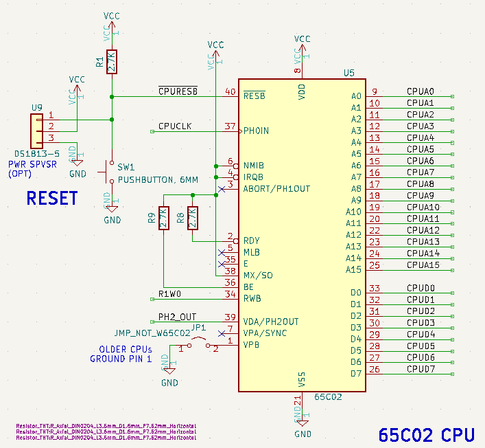
CPU
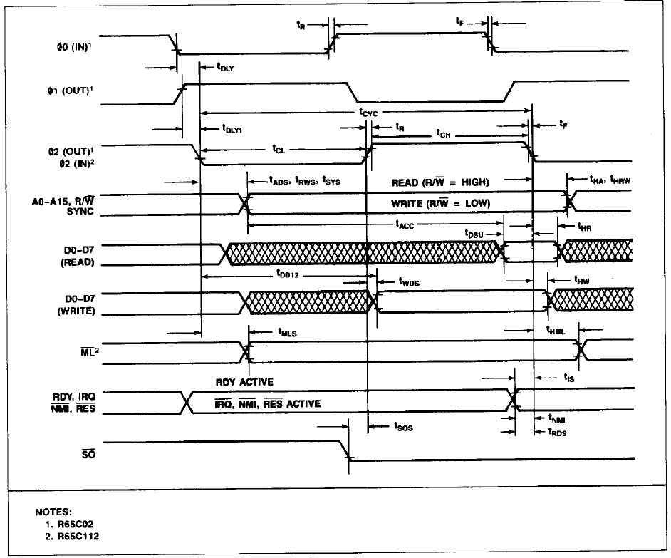
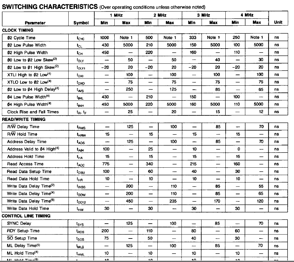
R6502 CPU Timing
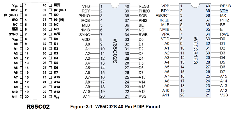
R65C02 vs W65C02 vs W65C816 CPUs
| U5 Pin | U5 Pin Name | Sig Name | Pullup | R65C02 sig | W65C02 sig | W65C816 sig |
|---|---|---|---|---|---|---|
| 1 | VSS/VPB | JP1 GNDs | N | VSS (IN) | VPB (OUT) | VPB (OUT) |
| 3 | PH1OUT/ABORT | NC | N | PH1OUT (OUT) | PH1OUT (OUT) | ABORT (IN) |
| 5 | NC/MLB | NC | N | NC | MLB (OUT) | MLB (OUT) |
| 7 | SYNC/VPA | NC | N | SYNC (OUT) | SYNC (OUT) | VPA (OUT) |
| 35 | NC/E | NC | N | NC | NC | EM/NAT (OUT) |
| 36 | NC/BE | Pull up | Y | NC | BE (IN) | BE (IN) |
| 37 | PH0IN/PH2IN | CPUCLK | N | PH0IN | PH2IN | PH2IN |
| 38 | SO/MX | VCC | VCC | SO* (IN) | SOB (IN) | MX (OUT) |
| 39 | PH2OUT/VDA | PH2_OUT | N | PH2OUT (OUT) | PH2OUT (OUT) | VDA(OUT) |
- Need to lift U5-38 to use W65C816 CPU
VDA/VPA (65C816)
- VDA/VPA
- 00, Internal operation (invalid address bus)
- 01, Valid Program Address
- 10, Valid Data Address
- 11, Opcode-fetch
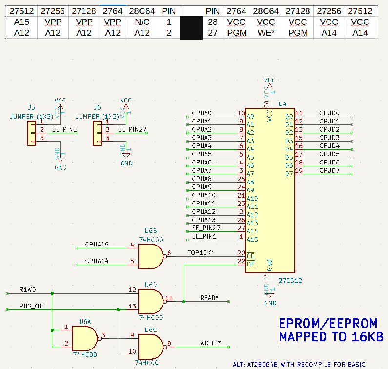
EPROM/EPROM
SRAM
Clock (Rev 1)
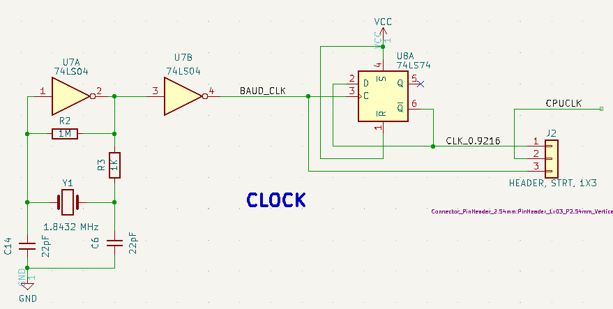
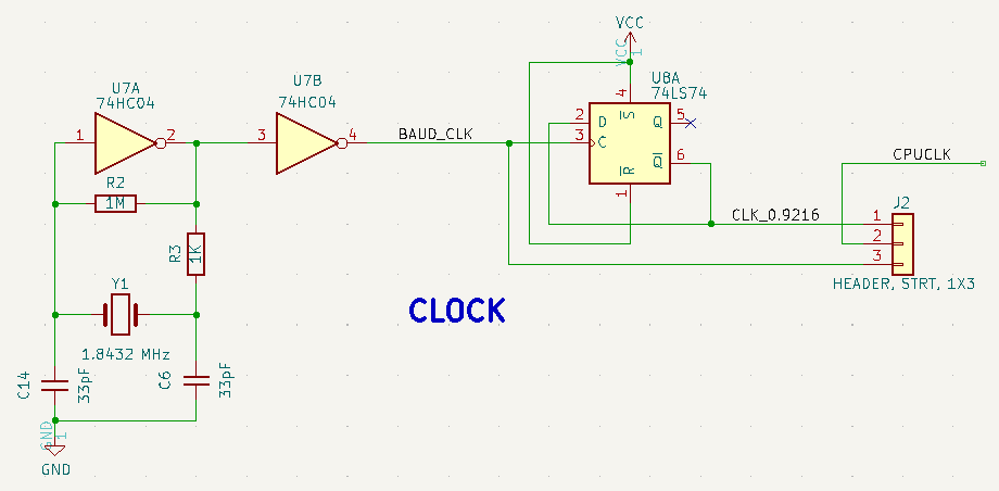
Clock (Rev 2)
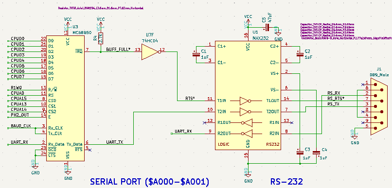
UART
- Can only use RS-232 or FTDI - one at a time
- Put MAX232 in a socket if you want flexibility
- Remove MAX232 if you want to use FTDI
FTDI
- Does not match Grant's pinout
- Can only use RS-232 or FTDI - one at a time
Headers / Connectors
J1 - RS-232 Serial
- DB-9 Male
- Matches Grant's pinout
- Pinout
- N/C
- Receive
- Transmit
- Loop to pin 6
- GND
- Loop to pin 4
- RTS
- N/C
- N/C
J2 - Speed Select Jumper
- 1-2 - 0.92 MHz
- 2-3 = 1.8432 MHz
J3 - FTDI / TTL Serial
- Requires a FTDI cross-over cable
- GND
- RTS* (out)
- +5V
- Receive (in)
- Transmit (out)
- N/C
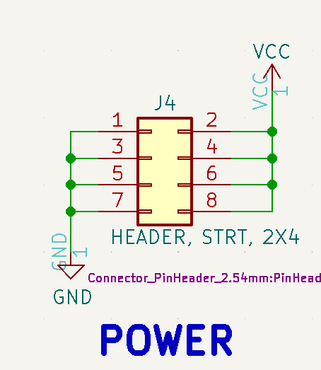
J4 - 5V Power
- 2x4 header
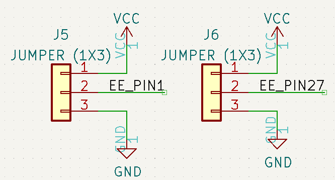
J5 / J6 - EPROM/EEPROM Select Jumpers
- J5 - EPROM Pin 1 jumper
- 1-2 for 28C64, 28C256 (Pull WE to VCC)
- 2-3 for 27256, 27SF256, 27512 (Pull A14 to GND)
- J6 - EPROM Pin 27 jumper
- GND (2-3)
EEPROM Pin Table
| 27512 | 27256 | 27SF256 | 28C256 | 27128 | 2764 | 28C64 | PIN | PIN | 2764 | 28C64 | 27128 | 28C256 | 27SF256 | 27256 | 27512 | |
|---|---|---|---|---|---|---|---|---|---|---|---|---|---|---|---|---|
| A15 | VPP | VPP | A14 | VPP | VPP | N/C | 1 | 28 | VCC | VCC | VCC | VCC | VCC | VCC | VCC | |
| A12 | A12 | A12 | A12 | A12 | A12 | A12 | 2 | 27 | PGM | WE* | PGM | WE* | A14 | A14 | A14 | |
| A7 | A7 | A7 | A7 | A7 | A7 | A7 | 3 | 26 | A13 | N/C | A13 | A13 | A13 | A13 | A13 | |
| A6 | A6 | A6 | A6 | A6 | A6 | A6 | 4 | 25 | A8 | A8 | A8 | A8 | A8 | A8 | A8 | |
| A5 | A5 | A5 | A5 | A5 | A5 | A5 | 5 | 24 | A9 | A9 | A9 | A9 | A9 | A9 | A9 | |
| A4 | A4 | A4 | A4 | A4 | A4 | A4 | 6 | 23 | A11 | A11 | A11 | A11 | A11 | A11 | A11 | |
| A3 | A3 | A3 | A3 | A3 | A3 | A3 | 7 | 22 | OE* | OE* | OE* | OE* | OE* | OE* | OE* | |
| A2 | A2 | A2 | A2 | A2 | A2 | A2 | 8 | 21 | A10 | A10 | A10 | A10 | A10 | A10 | A10 | |
| A1 | A1 | A1 | A1 | A1 | A1 | A1 | 9 | 20 | CE* | CE* | CE* | CE* | CE* | CE* | CE* | |
| A0 | A0 | A0 | A0 | A0 | A0 | A0 | 10 | 19 | D7 | D7 | D7 | D7 | D7 | D7 | D7 | |
| D0 | D0 | D0 | D0 | D0 | D0 | D0 | 11 | 18 | D6 | D6 | D6 | D6 | D6 | D6 | D6 | |
| D1 | D1 | D1 | D1 | D1 | D1 | D1 | 12 | 17 | D5 | D5 | D5 | D5 | D5 | D5 | D5 | |
| D2 | D2 | D2 | D2 | D2 | D2 | D2 | 13 | 16 | D4 | D4 | D4 | D4 | D4 | D4 | D4 | |
| GND | GND | GND | GND | GND | GND | GND | 14 | 15 | D3 | D3 | D3 | D3 | D3 | D3 | D3 |
JP1 - CPU Pin 1
- Install if CPU is not a WDC 65C02 or WDC 65C816
Software
- Link to Grant's files
- Source code
- osi_bas.s <== the Microsoft OSI BASIC and I/O routines SOURCE all in a single file
- Grant's I/O routines are at the end of it
- Files to allow the source to be assembled on a Windows based machine
- assemble.bat <== double click to assemble osi_bas.s and link to binary file "osi_bas.bin"
- This should be exactly 16K
- osi_bas.cfg <== configuration file for the linker (ensure ORG and entries in this file match if you change any)
- ca65.exe <== the assembler from the cc65 package. Use this. The new version on the cc65 site crashes!
- ld65.exe <== linker from the cc65 package
- Output files
- osi_bas.bin <== the ROM fine in pure binary
- osi_bas.lst <== Assembly listing file
- rom.hex <== the ROM fine in standard INTEL-HEX format
- To allow simple re-assembly, extract all files to the same folder
- Freeware utilities are available to convert the "bin" file to HEX or s19 (etc) - use your internet search tool to find
- All source code, assembler binaries and the HEX dump of the ROM is here
- It is in standard INTEL-HEX format for uploading to a suitable programmer.
First Unit Checkout (Rev 1 PCB)
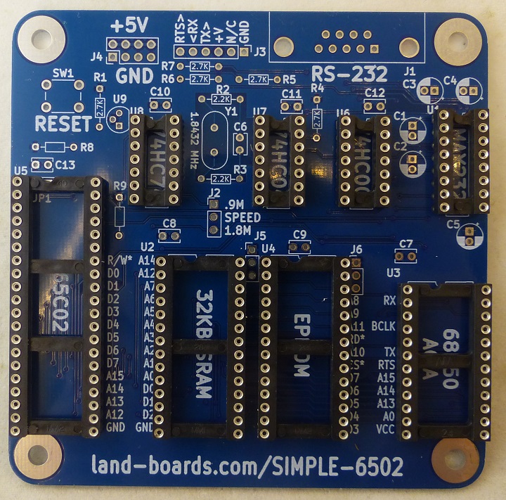
Install Sockets
- Machined pin sockets
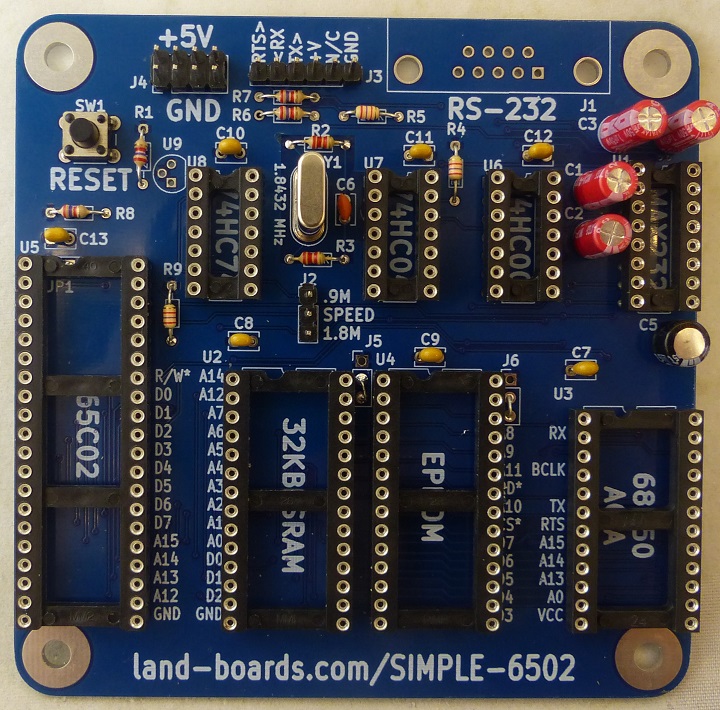
Install Passives
Power
- Install 2x4 at J4
- Power card via J4 with 5V
- Check power pins on parts
Clock
- Install Clock parts
- Did not have 270 pF cap, used 220 pF
- U7 (74HC04)
- Y1 1.8432 MHz crystal
- Clock "doubling" with 74HC04 part
- Worse with 74HC14
- Switched to 74LS04 - works well
- Install clock divider
- U8 (74HC74)
- Check clocks at J2
- Pin 1 s/b 0.9216 MHz
- Pin 3 s/b 1.8432 MHz
- Outputs are OK
- Need to change P/L and S/S to 74LS04
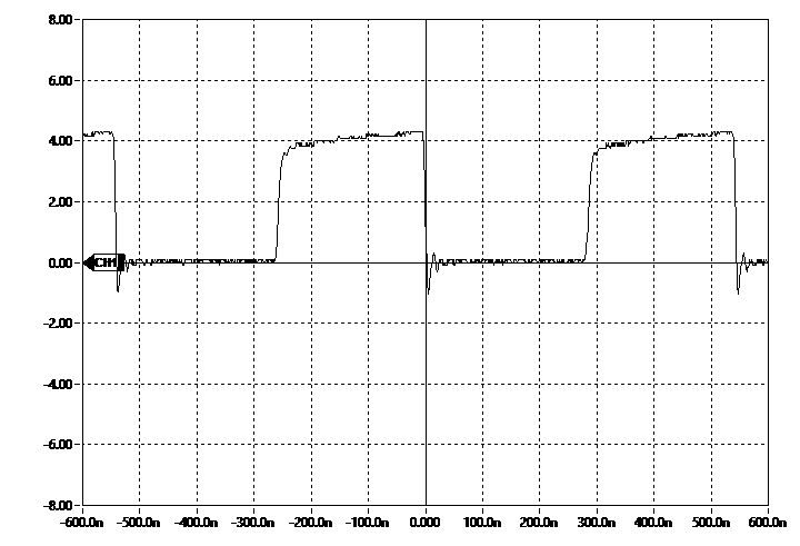
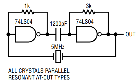
- Clock does not start up reliably
- Replaced part values with Fig 1d AN12 Circuit Techniques for Clock Sources
- Used 1nF cap instead of 1200pF
- Starts reliably but has a glitch
- Seems to run OK
- Reset is weird, sometimes does not boot and takes a couple of presses
- Not sure if this is clock related
- Order new 74LS04 parts
- See Rev 2 updates
Reset
- Install U9
- Install pushbutton switch SW1
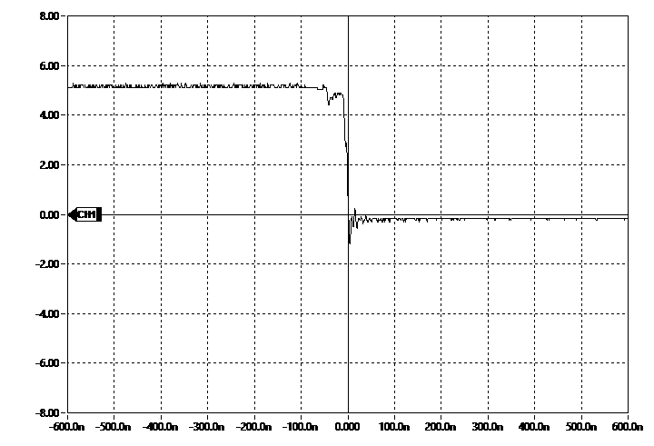
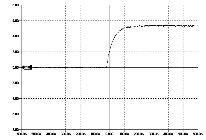
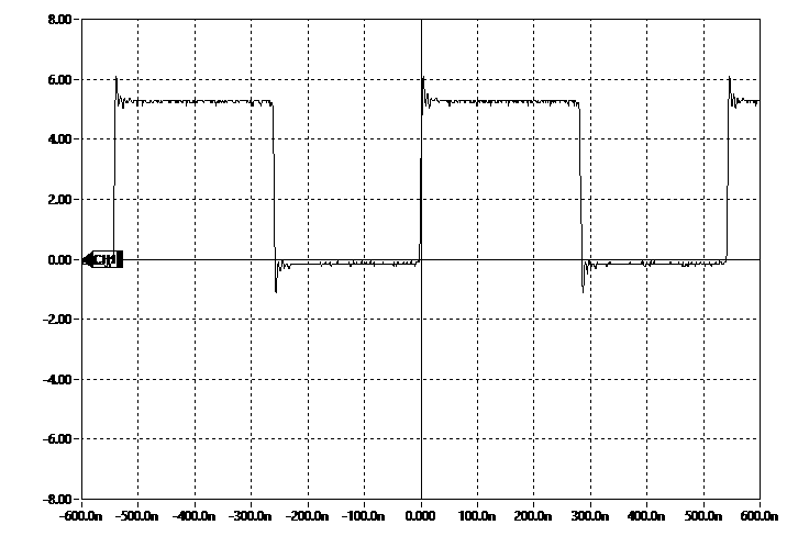
- Reset button gets stretched by Power Monitor U9
- Measure at 6502 U5 pin 40
- Falling edge scope cap
- Rising edge scope cap
- Switch failed, replaced - works
EPROM
- SST27C256 EEPROM
- 32 KB part
- Using first 16KB of EEPROM
- J5 EEPROM pin 1 = VPP = VCC or GND
- Jumper J5:2-3
- J6 EEPROM pin 27 = A14 = GND
- Jumper J6:2-3
- U1 - Do not install MAX232
- Use FTDI connector with FTDI-49MM card
- R65C02 CPU
- Install JP1 on rear of card as wire
EEPROM Programming
- Program using TL-866ii plus programmer
- File = ROM.hex
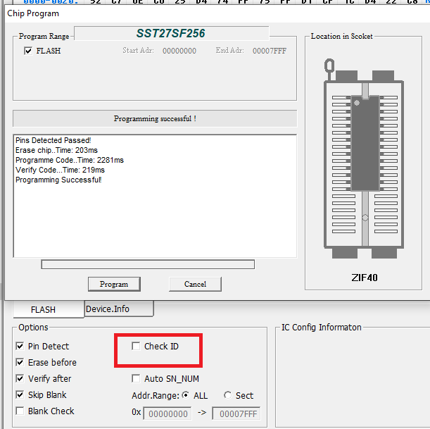
- Got Device ID error
- Turn off ID check
- Device programmed/verified
Install CPU, ROM, RAM, ACIA
- Do not install MAX232 yet
- Use FTDI connector with FTDI-49MM card
Test FTDI Serial
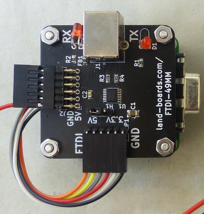
- Wiring is not 1:1 to FTDI-49MM
- Wire FTDI J3 to FTDI-49MM card
- Hardware handshake doesn't work with FTDI-49MM card
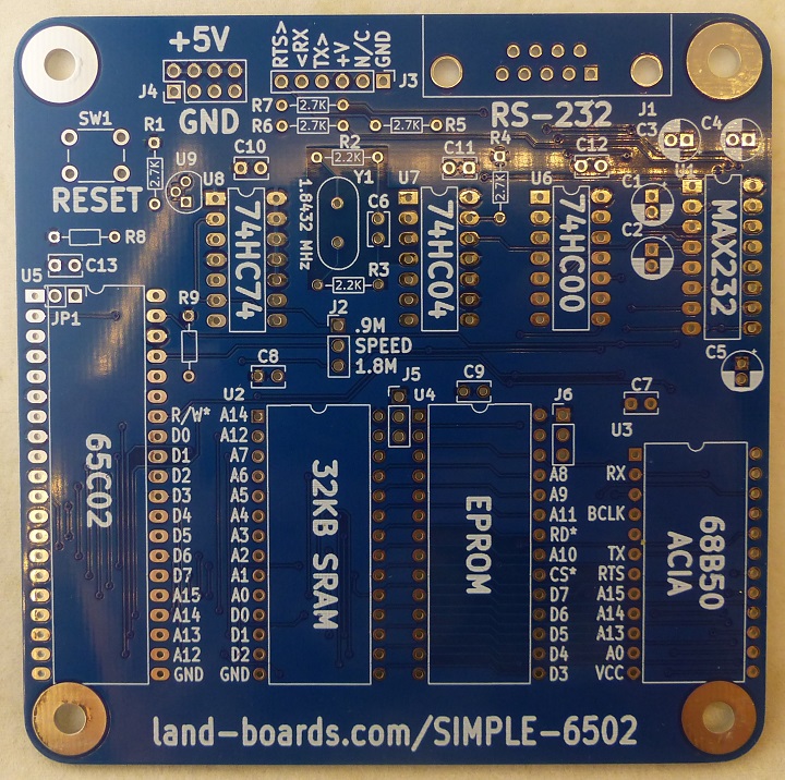
Card Without MAX232
- With DB-9 connector
- Install DB-9 Male
- Holes don't line up well, but 4-40 screws can fit
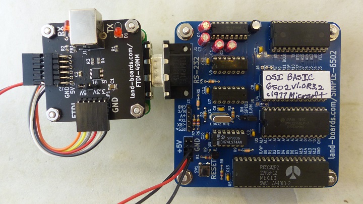
- Without MAX232
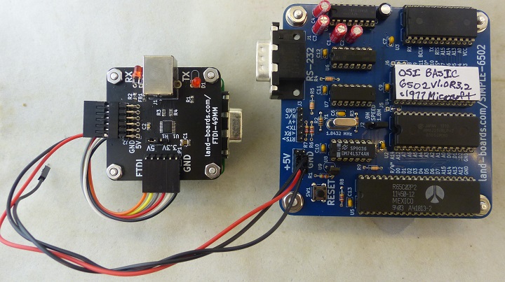
Built Card
- DB-9 connectors connected together
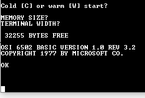
- Works
Performance
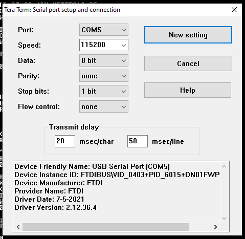
- TeraTerm settings
- Test software
10 FOR I =1 TO 10000
20 PRINT I
30 NEXT I
- Time ~38 secs
Mechanicals
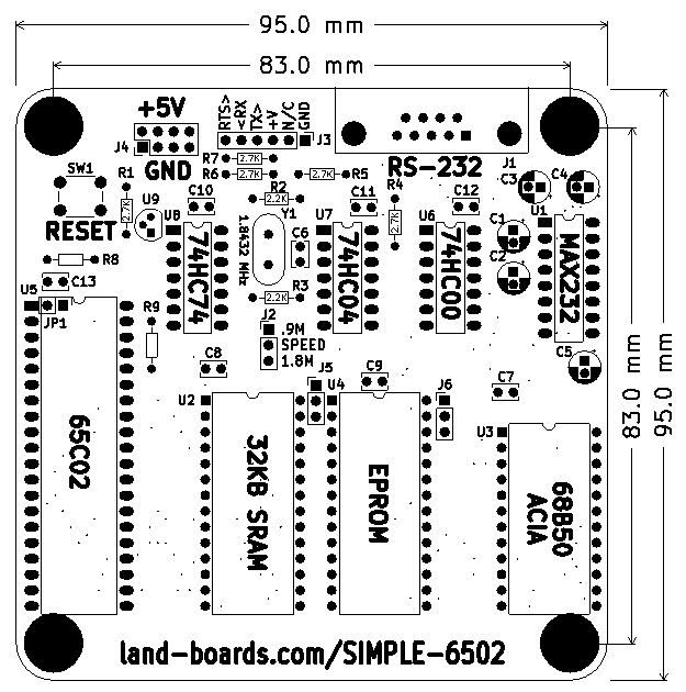
- Rev 1 board
- Rev 2 board has the same mechanical dimensions, but some parts are different
PCB Issues
Rev 2
- See clock section above for issues found during Rev 1 board checkout
- R8, R9 missing 2.7K marking on silkscreen
- Updated on Rev 2 interactive BOM
- C6, C14 change value to 33 pF
- Symptom with 22 pF caps was wrong oscillation frequency (approx 2.1 MHz)
- Crystal is 18pF
- Matching caps should be 2x (since the caps are essentially in series
- 36pF would be right, but there's also pin and PCB capacitance so use 33 pF caps
- U7 has to be 74HC04 with these other value parts
- Measured oscillator circuit timing/voltages
Rev 1
- Clocking not optimal - see notes above in clock section for debug issues
Assembly Sheet
Assembly Sheet Rev 2
- SIMPLE-6502 Rev 2 Interactive BOM
- Install jumper JP1 on rear of board if CPU is not a WDC 65C02 or WDC 65C816
- Install jumpers J5-2 to -3 and J6-2 to -3
- Clock changes from Grant's design
- U7 is 74HC04 (silkscreen shows 74LS04)
- 74LS04 might work if the Resistor values in the clock circuit are changed
- Jumper J2 clock to run the CPU at either 1.8432 MHz or half speed 0.9216 MHz

