Difference between revisions of "Z80 in 3 Chips"
Jump to navigation
Jump to search
Blwikiadmin (talk | contribs) |
Blwikiadmin (talk | contribs) |
||
| Line 55: | Line 55: | ||
=== J1 - USB B === | === J1 - USB B === | ||
| + | |||
| + | * Power and USB/Serial | ||
=== J2, J3 - I/O Ports === | === J2, J3 - I/O Ports === | ||
Revision as of 12:20, 6 September 2022
Contents
Features
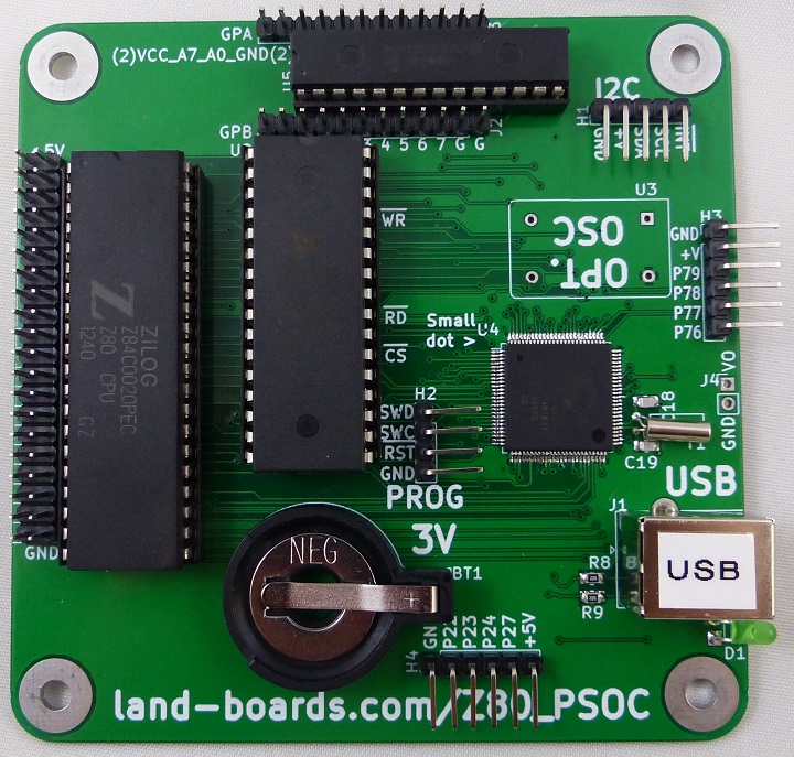
- Z80
- 12.5 MHz operation
- 512KB SRAM
- PSoC5LP
- PSoC5 LP emulates standard Z80 peripheral chips
- Serial port with USB
- Memory Management Unit (MMU)
- Controls 512KB SRAM
- Loader moves EPROM code to SRAM
- PSoC5 LP emulates standard Z80 peripheral chips
- Optional MCP23017 16-bit port expander
- I2C Addresses 0x24
- Optional Front Panel
- I2C Addresses 0x20-0x23
- SPI interface for SDHC card
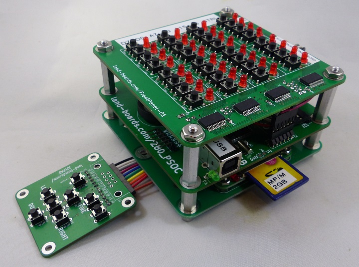
Stackup (top to bottom)
- Front Panel For 8 Bit Computers
- 32 LEDs
- 32 pushbutton switches
- I2C interface
- Z80 in 3 Chips (this card)
- SD_CARD_X49 mounted on CARRIER95TO49MM
- JOYPAD
Connectors
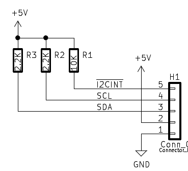
H1 - I2C Interface
- Connects to Front Panel Card via I2C
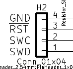
H2 - ISP Download
- Connects to PSoC programmer
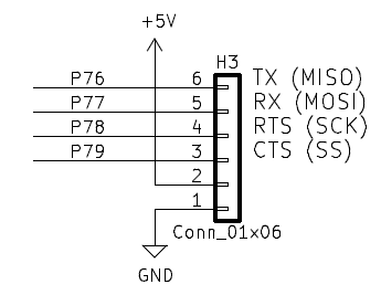
H3- SD Card
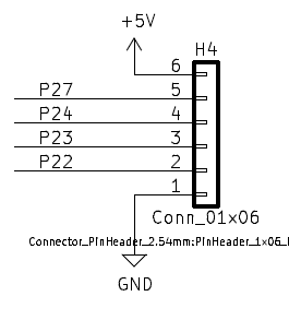
H4 - I/O
J1 - USB B
- Power and USB/Serial
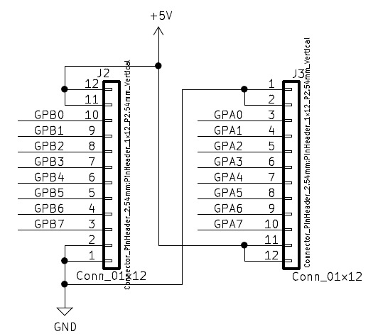
J2, J3 - I/O Ports
- J3 connects to JOYPAD
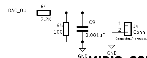
J4 - Audio Out
- DAC is the Analog function generator in the PSoC
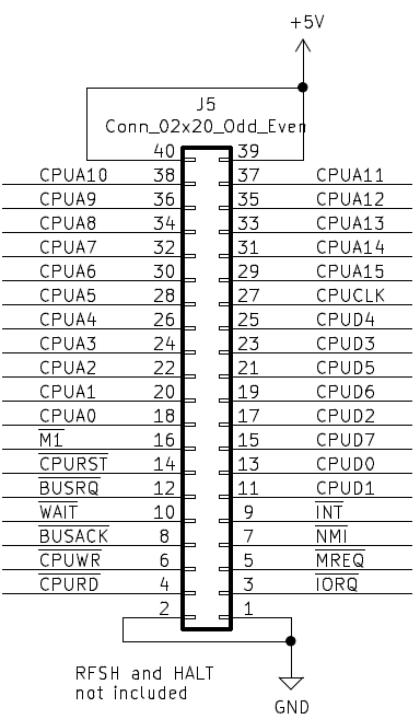
J5 - Z80 Signals
Software
- PSoC Code Github repo
- Z80 NASCOM BASIC
- CP/M Multiboot - Runs MultiComp 512KB SRAM version
- CP/M 2.2, CP/M 3.0, BASIC
- SBC-2G-512 on Retrobrewing site - Original author
- GitHub copy of SBC-2G-512
- Z80 Reference Designs
Hackaday Page
Videos
