Difference between revisions of "SIMPLE-Z80"
Jump to navigation
Jump to search
Blwikiadmin (talk | contribs) |
Blwikiadmin (talk | contribs) |
||
| Line 460: | Line 460: | ||
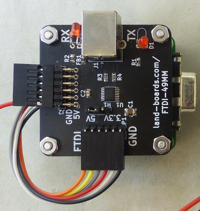
** [[DCE]] has female DB-9 | ** [[DCE]] has female DB-9 | ||
** Separate power cable J2 on [[FTDI-49MM]] to J3 on card | ** Separate power cable J2 on [[FTDI-49MM]] to J3 on card | ||
| + | |||
| + | [[FILE:FTDI_DCE_P1090192-720PXV.jpg]] | ||
| + | |||
* Works | * Works | ||
Revision as of 12:46, 2 March 2023
Contents
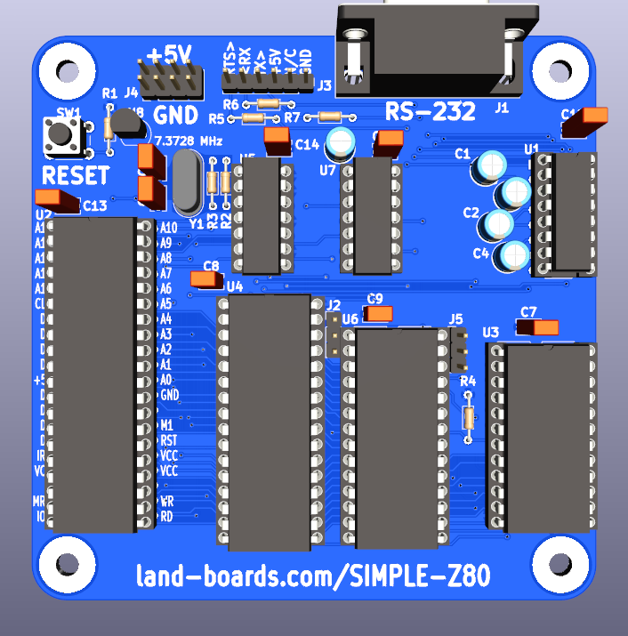
Features
- Build of Grant Searles's Simple Z80 CPU
- Runs BASIC
- Z80 CPU
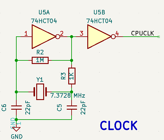
- 7.3728 MHz clock
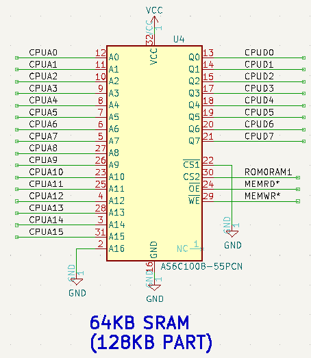
- 56KB SRAM (uses 128KB parts)
- 8KB EPROM/EEPROM
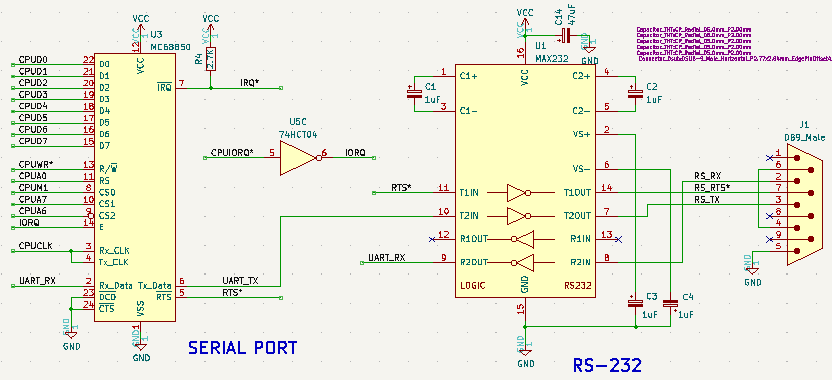
- 68B50 Serial Port (ACIA)
- RS-232 port
- Header for FTDI
- 115,200 baud
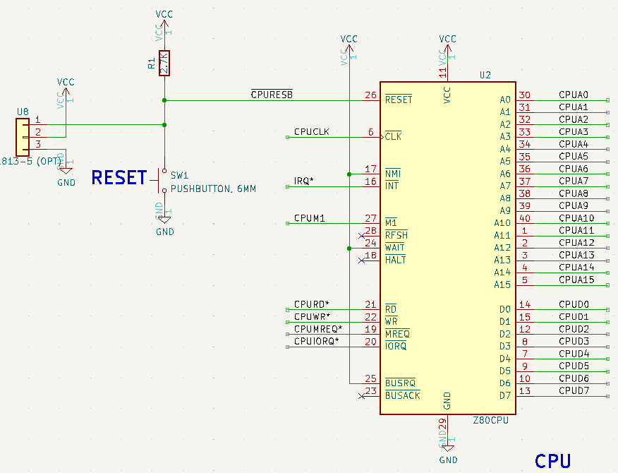
- Reset switch with optional DS1813 Power Supervisor
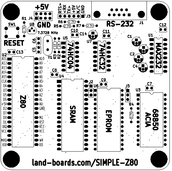
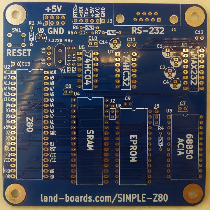
- 95x95mm card
- (4) 6-32 mounting holes
Memory Map
- 0x0000-0x1FFF 8KB ROM
- 0x2000-0xFFFF 56KB SRAM
- I/O
- 0x00-0x7F - Free
- 0x80-0x81 - Serial port (ACIA)
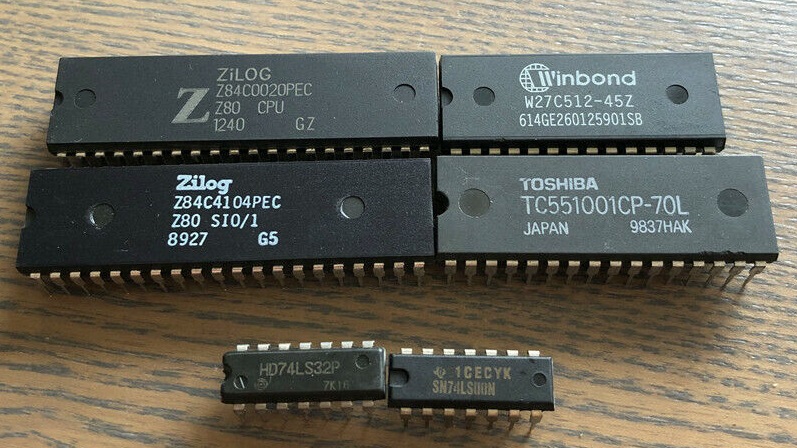
Chip Set
- Ebay listing
- Needs 68B50 to run Grant's code
Design
- CPU
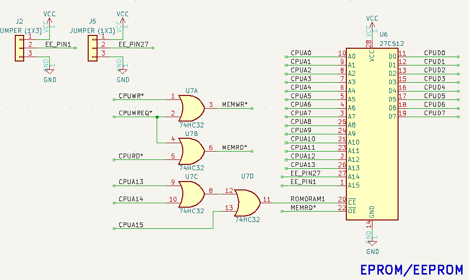
- EPROM
- SRAM
- ACIA
- Clock
Headers / Connectors
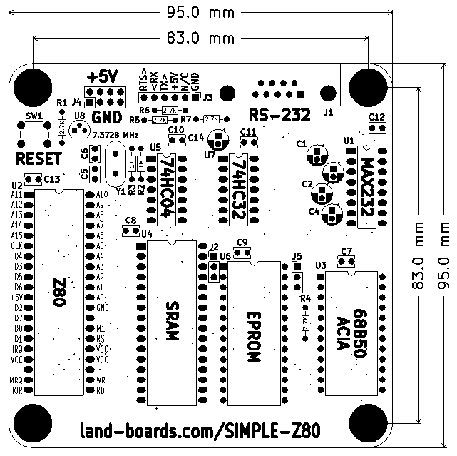
J1 - RS-232 Serial
- DB-9 Male
- Pinout
- N/C
- Receive
- Transmit
- Loop to pin 6
- GND
- Loop to pin 4
- RTS
- N/C
- N/C
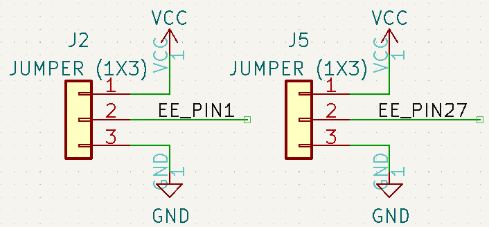
J2/J5 - EPROM/EEPROM Select Jumpers
EEPROM Pin Table
| 27512 | 27256 | 27SF256 | 28C256 | 27128 | 2764 | 28C64 | PIN | PIN | 2764 | 28C64 | 27128 | 28C256 | 27SF256 | 27256 | 27512 | |
|---|---|---|---|---|---|---|---|---|---|---|---|---|---|---|---|---|
| A15 | VPP | VPP | A14 | VPP | VPP | N/C | 1 | 28 | VCC | VCC | VCC | VCC | VCC | VCC | VCC | |
| A12 | A12 | A12 | A12 | A12 | A12 | A12 | 2 | 27 | PGM | WE* | PGM | WE* | A14 | A14 | A14 | |
| A7 | A7 | A7 | A7 | A7 | A7 | A7 | 3 | 26 | A13 | N/C | A13 | A13 | A13 | A13 | A13 | |
| A6 | A6 | A6 | A6 | A6 | A6 | A6 | 4 | 25 | A8 | A8 | A8 | A8 | A8 | A8 | A8 | |
| A5 | A5 | A5 | A5 | A5 | A5 | A5 | 5 | 24 | A9 | A9 | A9 | A9 | A9 | A9 | A9 | |
| A4 | A4 | A4 | A4 | A4 | A4 | A4 | 6 | 23 | A11 | A11 | A11 | A11 | A11 | A11 | A11 | |
| A3 | A3 | A3 | A3 | A3 | A3 | A3 | 7 | 22 | OE* | OE* | OE* | OE* | OE* | OE* | OE* | |
| A2 | A2 | A2 | A2 | A2 | A2 | A2 | 8 | 21 | A10 | A10 | A10 | A10 | A10 | A10 | A10 | |
| A1 | A1 | A1 | A1 | A1 | A1 | A1 | 9 | 20 | CE* | CE* | CE* | CE* | CE* | CE* | CE* | |
| A0 | A0 | A0 | A0 | A0 | A0 | A0 | 10 | 19 | D7 | D7 | D7 | D7 | D7 | D7 | D7 | |
| D0 | D0 | D0 | D0 | D0 | D0 | D0 | 11 | 18 | D6 | D6 | D6 | D6 | D6 | D6 | D6 | |
| D1 | D1 | D1 | D1 | D1 | D1 | D1 | 12 | 17 | D5 | D5 | D5 | D5 | D5 | D5 | D5 | |
| D2 | D2 | D2 | D2 | D2 | D2 | D2 | 13 | 16 | D4 | D4 | D4 | D4 | D4 | D4 | D4 | |
| GND | GND | GND | GND | GND | GND | GND | 14 | 15 | D3 | D3 | D3 | D3 | D3 | D3 | D3 |
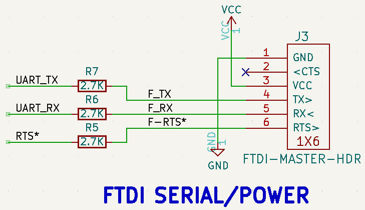
J3 - FTDI / TTL Serial
- GND
- N/C
- +5V
- Transmit (out)
- Receive (in)
- RTS* (out)
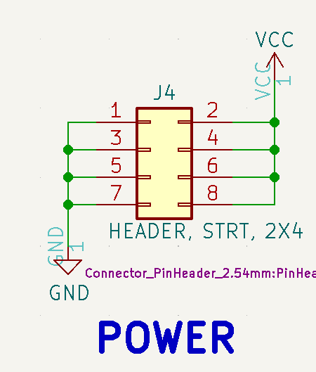
J4 - 5V Power
- 2x4 header
First Unit Checkout
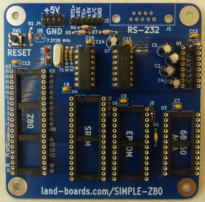
- PCB
Install Sockets
- Machined pin sockets
Install Passives
Power
- Install 2x4 at J4
- Power card via J4 with 5V
- Check power pins on parts
Clock
- Install Clock parts
- Install R2, R3
- Install C5, C6
- Install 7.3728 MHz crystal
- Install 74HC04 at U5
- Measure clock at U5-4
- 7.32 MHz clock - looks good
Reset
- Do not install U8 Power Monitor
- Reset button gets stretched by Power Monitor U9
- Install pushbutton switch SW1
- Measure reset at Z80 U2 pin marked RST on silkscreen
EPROM
- U6 = SST27C256 EEPROM
- 32 KB part
- Using first 16KB of EEPROM
- J2 EEPROM pin 1 = VPP = VCC or GND
- Jumper J2:2-3
- J5 EEPROM pin 27 = A14 = GND
- Jumper J5:2-3
EEPROM Programming
- Program using TL-866ii plus programmer
- File = ROM.HEX - I/O routines plus BASIC
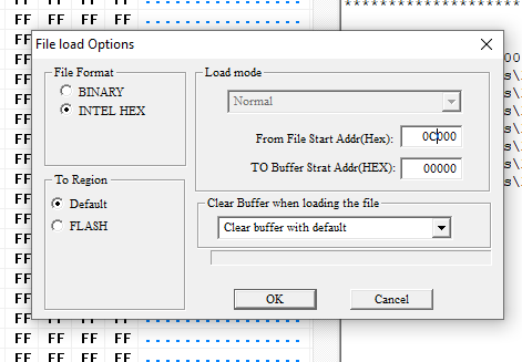
- Set offsets for 27SF256 part
- Part is 32 KB
- hex files is 16 KB
- Set From File Start Addr(Hex) to 00000
- To Buffer Start Addr(Hex) to 00000
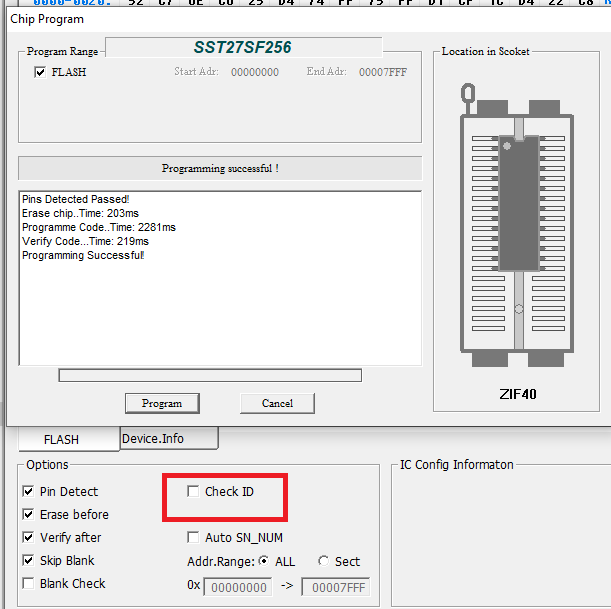
- Got Device ID error
- Turn off ID check
- Device programmed/verified
Install CPU, ROM, RAM, ACIA
- U1 - Do not install MAX232 yet
- Use FTDI connector with FTDI-49MM card
Test FTDI Serial
Test RS-232 Serial
- With MAX232
- Install DB-9 Male
- Holes don't line up well, but 4-40 screws can fit
- Connected to FTDI-49MM and DCE cards
- Works
Software
- ROM.HEX - ROM file
- Nascom Computer BASIC modified to remove all hardware-specific code
Source files
- intmini.asm - the interupt driven mini startup program needed to boot into BASIC
- basic.asm - BASIC 4.7b - a conversion of Microsoft BASIC 4.7, as used on the Nascom computers (see below for details)
Output files
- INTMINI.HEX
- BASIC.HEX
- ROM.HEX - the complete 8K ROM ready for burning to an EPROM - the unused contents are filled with FF values.
- Within the ROM, the serial handler is first (starting at address 0000H), followed by the BASIC interpreter (starting at 0100H).
Assembler files (for Windows/DOS)
- _ASSEMBLE.BAT - double-click in Windows to run the assembly if needed
- TASM.EXE
- TASM80.TAB
Acknowledgements
- BASIC is Microsoft BASIC 4.7 for the NASCOM, heavily modified by Grant to remove references to different monitors, screen handlers and keyboard matrix reading
- TASM assembler is a partial distribution of the package from Speech Technology Incorporated
