Difference between revisions of "UNI-OPAMP-08"
Jump to navigation
Jump to search
Blwikiadmin (talk | contribs) |
Blwikiadmin (talk | contribs) |
||
| (17 intermediate revisions by the same user not shown) | |||
| Line 1: | Line 1: | ||
| − | [[File:tindie-mediums.png|link=https://www.tindie.com/products/land_boards/ | + | [[File:tindie-mediums.png|link=https://www.tindie.com/products/land_boards/universal-op-amp-card-uni-opamp-08/]] |
| + | |||
| + | == Eight Channel Universal Op Amp == | ||
[[File:UNI-OPAMP-08_6122-512pxV.jpg]] | [[File:UNI-OPAMP-08_6122-512pxV.jpg]] | ||
| Line 9: | Line 11: | ||
* 8 Channels | * 8 Channels | ||
* 2 Quad OpAmps | * 2 Quad OpAmps | ||
| − | ** LM324 parts (typical) in SOIC-14 package | + | ** [https://www.onsemi.com/pub/Collateral/LM324-D.PDF LM324] parts (typical) in SOIC-14 package |
| − | ** Also supports lower voltage op amps such as MCP6004 | + | *** 3V to 32V |
| + | ** Also supports lower voltage op amps such as [https://www.microchip.com/wwwproducts/en/MCP6004 MCP6004] | ||
| + | *** 1.8V to 6V | ||
** SMT parts | ** SMT parts | ||
* Individual 4-pin headers per channel | * Individual 4-pin headers per channel | ||
| Line 17: | Line 21: | ||
* 49X49mm form factor | * 49X49mm form factor | ||
* (4) 4-40 mounting holes | * (4) 4-40 mounting holes | ||
| + | |||
| + | == Connectors == | ||
| + | |||
| + | [[File:UNI-OPAMP-08_Conn.PNG]] | ||
== Configurations == | == Configurations == | ||
| + | |||
| + | * The reference designs (below) are for the first channel. | ||
| + | |||
| + | [[File:OpAMP-sch - 787px.PNG]] | ||
| + | |||
| + | * The resistor mapping from the first channel on the schematic to the other channels are as follows. | ||
| + | |||
| + | === Resistors === | ||
| + | |||
| + | {| class="wikitable" | ||
| + | !OpAmp | ||
| + | !Ax-/Ix- | ||
| + | !Ax+/Ix+ | ||
| + | !Ax-/Qx | ||
| + | !Ax-/Gnd | ||
| + | !Ax+/Gnd | ||
| + | |- | ||
| + | |U1A | ||
| + | |R1 | ||
| + | |R2 | ||
| + | |R3 | ||
| + | |R4 | ||
| + | |R5 | ||
| + | |- | ||
| + | |U1B | ||
| + | |R6 | ||
| + | |R7 | ||
| + | |R8 | ||
| + | |R10 | ||
| + | |R9 | ||
| + | |- | ||
| + | |U1C | ||
| + | |R11 | ||
| + | |R12 | ||
| + | |R13 | ||
| + | |R14 | ||
| + | |R15 | ||
| + | |- | ||
| + | |U1D | ||
| + | |R16 | ||
| + | |R17 | ||
| + | |R18 | ||
| + | |R20 | ||
| + | |R19 | ||
| + | |- | ||
| + | |U2A | ||
| + | |R23 | ||
| + | |R24 | ||
| + | |R25 | ||
| + | |R21 | ||
| + | |R22 | ||
| + | |- | ||
| + | |U2B | ||
| + | |R28 | ||
| + | |R29 | ||
| + | |R30 | ||
| + | |R27 | ||
| + | |R26 | ||
| + | |- | ||
| + | |U2C | ||
| + | |R33 | ||
| + | |R34 | ||
| + | |R35 | ||
| + | |R31 | ||
| + | |R32 | ||
| + | |- | ||
| + | |U2D | ||
| + | |R38 | ||
| + | |R39 | ||
| + | |R40 | ||
| + | |R37 | ||
| + | |R36 | ||
| + | |- | ||
| + | |} | ||
| + | |||
| + | == Reference Designs == | ||
* Reference drawings are from [https://www.ti.com/lit/an/snla140c/snla140c.pdf Ap Note 31] | * Reference drawings are from [https://www.ti.com/lit/an/snla140c/snla140c.pdf Ap Note 31] | ||
* Reference designators are for channel 1 | * Reference designators are for channel 1 | ||
| − | ** See [http://land-boards.com/UNI-OPAMP-08/UNI-OPAMP-08_Schematic.pdf schematic] for other channels | + | ** See resistor values table (above) [http://land-boards.com/UNI-OPAMP-08/UNI-OPAMP-08_Schematic.pdf schematic] for other channels |
=== Differential Amplifier === | === Differential Amplifier === | ||
| + | |||
| + | ==== Differential Amplifier - Reference Design ==== | ||
[[File:Ap31-OpAmp-DiffAmp.PNG]] | [[File:Ap31-OpAmp-DiffAmp.PNG]] | ||
| − | === Differential Amplifier Stuffing Options === | + | ==== Differential Amplifier Stuffing Options ==== |
[[File:OpAMP-DiffAmp.PNG]] | [[File:OpAMP-DiffAmp.PNG]] | ||
=== Current to Voltage Converter === | === Current to Voltage Converter === | ||
| + | |||
| + | ==== Current to Voltage Converter - Reference Design ==== | ||
[[File:Ap31-OpAmp-Curr2Volts.PNG]] | [[File:Ap31-OpAmp-Curr2Volts.PNG]] | ||
| − | === Voltage to Current Stuffing Options === | + | ==== Voltage to Current Stuffing Options ==== |
[[File:OpAMP-sch - Curr2Volts.PNG]] | [[File:OpAMP-sch - Curr2Volts.PNG]] | ||
| − | === Inverting Amplifier | + | === Inverting Amplifier === |
| + | |||
| + | ==== Inverting Amplifier - Reference Design ==== | ||
[[File:Ap31-OpAmp-InvAmp.PNG]] | [[File:Ap31-OpAmp-InvAmp.PNG]] | ||
| − | === Inverting Amplifier Stuffing Options === | + | ==== Inverting Amplifier Stuffing Options ==== |
[[File:OpAMP-sch - InvAmp.PNG]] | [[File:OpAMP-sch - InvAmp.PNG]] | ||
=== Non-inverting Amplifier === | === Non-inverting Amplifier === | ||
| + | |||
| + | ==== Non-inverting Amplifier - Reference Design ==== | ||
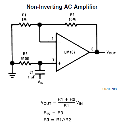
[[File:Ap31-OpAmp-NonInvAmp.PNG]] | [[File:Ap31-OpAmp-NonInvAmp.PNG]] | ||
| − | === Non-inverting Stuffing Options === | + | ==== Non-inverting Stuffing Options ==== |
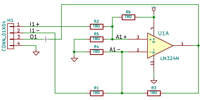
[[File:OpAMP-sch - NonInvAmp.PNG]] | [[File:OpAMP-sch - NonInvAmp.PNG]] | ||
Latest revision as of 19:22, 5 January 2020
Contents
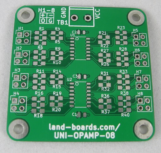
Eight Channel Universal Op Amp
Features
- Universal OpAmp Board
- Configurable for typical OpAmp circuits
- 8 Channels
- 2 Quad OpAmps
- Individual 4-pin headers per channel
- Terminal block for power
- Bypass capacitors
- 49X49mm form factor
- (4) 4-40 mounting holes
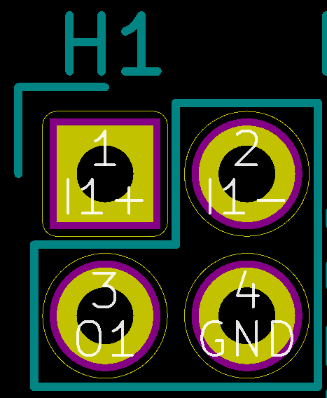
Connectors
Configurations
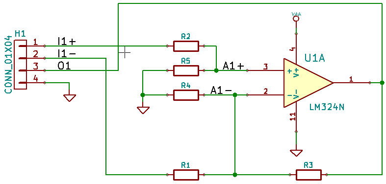
- The reference designs (below) are for the first channel.
- The resistor mapping from the first channel on the schematic to the other channels are as follows.
Resistors
| OpAmp | Ax-/Ix- | Ax+/Ix+ | Ax-/Qx | Ax-/Gnd | Ax+/Gnd |
|---|---|---|---|---|---|
| U1A | R1 | R2 | R3 | R4 | R5 |
| U1B | R6 | R7 | R8 | R10 | R9 |
| U1C | R11 | R12 | R13 | R14 | R15 |
| U1D | R16 | R17 | R18 | R20 | R19 |
| U2A | R23 | R24 | R25 | R21 | R22 |
| U2B | R28 | R29 | R30 | R27 | R26 |
| U2C | R33 | R34 | R35 | R31 | R32 |
| U2D | R38 | R39 | R40 | R37 | R36 |
Reference Designs
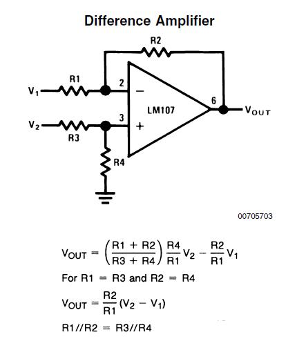
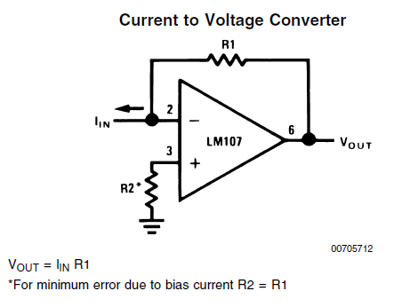
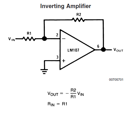
- Reference drawings are from Ap Note 31
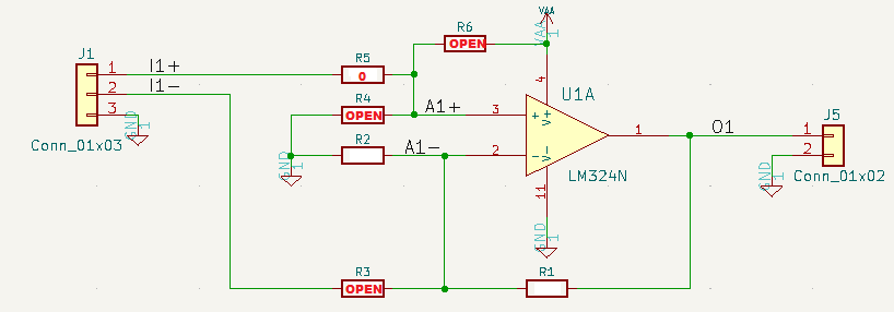
- Reference designators are for channel 1
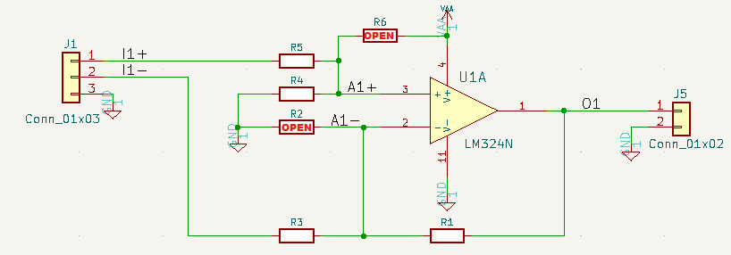
- See resistor values table (above) schematic for other channels

