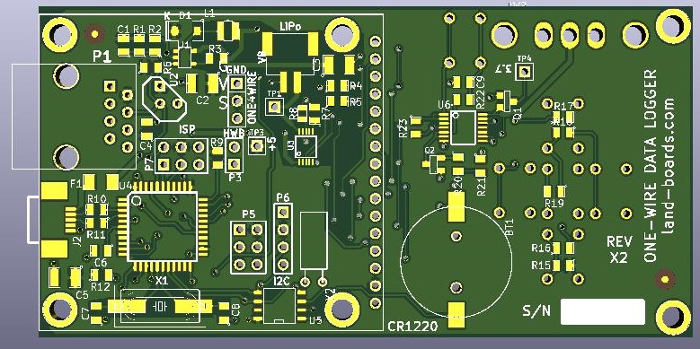
Difference between revisions of "One Wire Data Logger"
Jump to navigation
Jump to search
Blwikiadmin (talk | contribs) |
Blwikiadmin (talk | contribs) (→P5 ISP) |
||
| (17 intermediate revisions by the same user not shown) | |||
| Line 4: | Line 4: | ||
* One wire RJ-45 connector | * One wire RJ-45 connector | ||
| + | * ATMega32U4 Microprocessor | ||
| + | ** USB connector | ||
* 0.96" OLED | * 0.96" OLED | ||
| − | * | + | * LiPo battery |
| + | ** JST connector | ||
| + | ** Battery charger | ||
| + | * Real-time clock | ||
| + | ** Battery | ||
| + | * I2C connector | ||
| + | * Switching power regulator | ||
| + | |||
| + | == Connectors == | ||
| + | |||
| + | === J2 - USB-B === | ||
| + | |||
| + | === P1 - One wire RJ-45 === | ||
| + | |||
| + | === P3 HWB - Download === | ||
| + | |||
| + | === P5 ISP === | ||
| + | |||
| + | # MISO | ||
| + | # VCC | ||
| + | # SCK | ||
| + | # MOSI | ||
| + | # RST | ||
| + | # GND | ||
| + | |||
| + | === P6 I2C === | ||
| + | |||
| + | # GND | ||
| + | # VCC | ||
| + | # SDA | ||
| + | # SCL | ||
| + | |||
| + | === P7 - ADC pins === | ||
| + | |||
| + | # ADC4 | ||
| + | # ADC1 | ||
| + | # ADC5 | ||
| + | # VCC | ||
| + | # ADC6 | ||
| + | # GND | ||
| + | |||
| + | == Test Points == | ||
| + | |||
| + | === TP1 - Battery === | ||
| + | |||
| + | === TP2 === | ||
| + | |||
| + | === TP3 Switching power supply 5V output === | ||
| + | |||
| + | === TP4 Pin 3.7 === | ||
| + | |||
| + | * Switched power | ||
| + | |||
| + | == Switches == | ||
| + | |||
| + | === SW1 - Power override === | ||
| + | |||
| + | === Up/Down/Left/Right/Select === | ||
| + | |||
| + | == Software == | ||
| + | |||
| + | * [https://github.com/land-boards/lb-boards/tree/master/Projects/OneWireLogger Github] | ||
== Assembly Sheet == | == Assembly Sheet == | ||
* [[One Wire Data Logger Assembly Sheet]] | * [[One Wire Data Logger Assembly Sheet]] | ||
Latest revision as of 20:43, 5 January 2020
Features
- One wire RJ-45 connector
- ATMega32U4 Microprocessor
- USB connector
- 0.96" OLED
- LiPo battery
- JST connector
- Battery charger
- Real-time clock
- Battery
- I2C connector
- Switching power regulator
Connectors
J2 - USB-B
P1 - One wire RJ-45
P3 HWB - Download
P5 ISP
- MISO
- VCC
- SCK
- MOSI
- RST
- GND
P6 I2C
- GND
- VCC
- SDA
- SCL
P7 - ADC pins
- ADC4
- ADC1
- ADC5
- VCC
- ADC6
- GND
Test Points
TP1 - Battery
TP2
TP3 Switching power supply 5V output
TP4 Pin 3.7
- Switched power
