Difference between revisions of "RETRO-65C816"
Jump to navigation
Jump to search
Blwikiadmin (talk | contribs) |
Blwikiadmin (talk | contribs) |
||
| Line 6: | Line 6: | ||
** 3.3V | ** 3.3V | ||
** 8 MHz | ** 8 MHz | ||
| + | ** All pins are brought to FPGA | ||
| + | ** Address A0-A15 and Data lines also go directly to the SRAM | ||
| + | ** FPGA can have the ROM internally or download it to the SRAM | ||
* 1MB SRAM | * 1MB SRAM | ||
| + | ** 45nS access time | ||
* FTDI USB B | * FTDI USB B | ||
* VGA | * VGA | ||
| Line 13: | Line 17: | ||
** 5V KEYBOARD | ** 5V KEYBOARD | ||
** Level translator to 3.3V for FPGA | ** Level translator to 3.3V for FPGA | ||
| − | * SD card socket | + | * SD card socket |
| + | ** Full-sized SD | ||
* QMTECH FPGA card mounts on top | * QMTECH FPGA card mounts on top | ||
** [[QMTECH EP4CE15 FPGA Card]] | ** [[QMTECH EP4CE15 FPGA Card]] | ||
Revision as of 00:56, 30 May 2022
Features
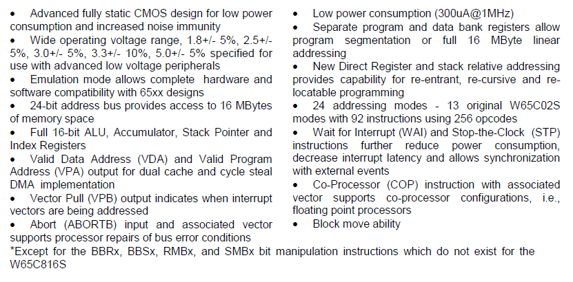
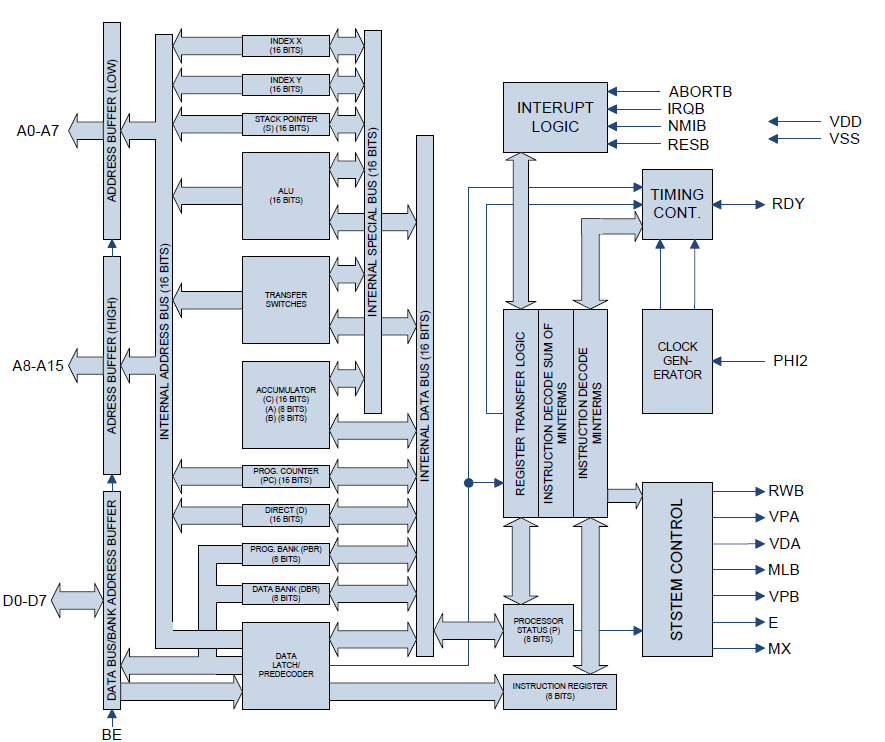
- 65C816 CPU
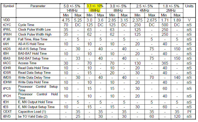
- 3.3V
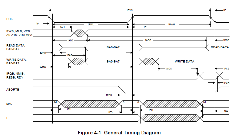
- 8 MHz
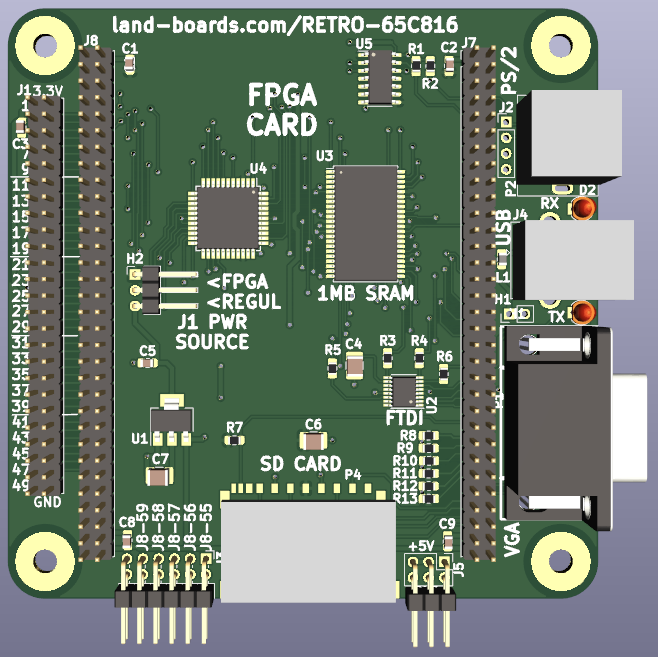
- All pins are brought to FPGA
- Address A0-A15 and Data lines also go directly to the SRAM
- FPGA can have the ROM internally or download it to the SRAM
- 1MB SRAM
- 45nS access time
- FTDI USB B
- VGA
- 2:2:2 R:G:B
- PS/2 keyboard
- 5V KEYBOARD
- Level translator to 3.3V for FPGA
- SD card socket
- Full-sized SD
- QMTECH FPGA card mounts on top
