Difference between revisions of "TinyDuino85"
Jump to navigation
Jump to search
Blwikiadmin (talk | contribs) |
Blwikiadmin (talk | contribs) |
||
| Line 45: | Line 45: | ||
== Mapping Arduino Pins to TinyDuino85 pins == | == Mapping Arduino Pins to TinyDuino85 pins == | ||
| − | + | <pre> | |
ATTiny85 Pin PWB Marking Arduino function | ATTiny85 Pin PWB Marking Arduino function | ||
1 P1-3 Reset | 1 P1-3 Reset | ||
| Line 53: | Line 53: | ||
6 D1 Digital Pin 1 | 6 D1 Digital Pin 1 | ||
7 D2 Digital Pin 2 | 7 D2 Digital Pin 2 | ||
| − | ATTiny85 Pinout.PNG | + | <pre> |
| + | |||
| + | [[File:ATTiny85 Pinout.PNG]] | ||
| − | ATtiny45-85.png | + | [[File:ATtiny45-85.png]] |
== X2 Improvements/Checkout == | == X2 Improvements/Checkout == | ||
Revision as of 14:40, 10 January 2020
Contents
TinyDuino85
Features
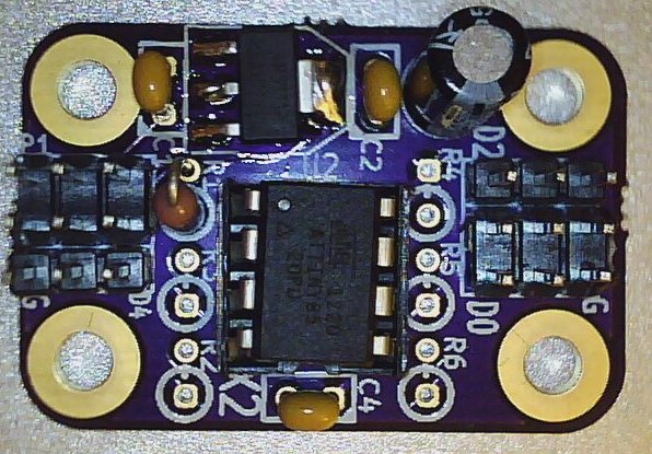
The current version of this board is Rev X2. This board is an ATTiny85 Arduino-Compatible GVS design. My first version of this card, TinyDuino85 Rev X1 was pretty good, but it had a few minor issues which this version corrects.
TinyDuino85 is an Atmel ATTiny85 based design. Distinctive features are:
- Four mounting holes - standard 4-40 hardware
- GVS Connectors for D0-D5 (5-lines)
- X2 version adds Reset pin to power connector for ease of downloading
- Installable resistors for pullups on lines (1-Wire or LDR sensors can be done easily)
- Small form factor card easily fits into small Altoids tin
- On-board +5V voltage regulator
- SMT regulator uses the top layer of the board as heat spreader
- Rounded corners on the PCB for easy mounting
Connectors
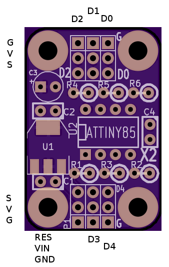
The mapping of connector pins to the Arduino signals are:
GVS Connectors
D0-D4 GVS connectors for each of the lines.
Pin	Description
1	Ground
2	Vcc
3	Signal
P1 Connector
The P1 connector brings power into the card (for use with the Voltage Regulator) and allows access of the reset line (needed for external programming).
Pin	Description
1	GND
2	VIN
3	RESET
Mapping Arduino Pins to TinyDuino85 pins
ATTiny85 Pin 	PWB Marking 	Arduino function
1 	P1-3	Reset
2 	D3	Digital Pin 3/Analog A3
3 	D4	Digital Pin 4/Analog A2
5 	D0	Digital Pin 0
6 	D1	Digital Pin 1
7	D2	Digital Pin 2
<pre>

[[File:ATTiny85 Pinout.PNG]]

[[File:ATtiny45-85.png]]

== X2 Improvements/Checkout ==

Reset line added to power pin and wiring for power in pin is set to be the same as GVS connectors
Bottom left corner mounting hole close spacing
Reduced footprint of big cap
Smaller board footprint
Application
My initial application is to use this in my Room Fan Controller design since that design only requires 2 inputs (from LDR Sensor and Temperature sensor) and one output (AC relay). The code fits into 8K of memory.

== Programming ==

[[File:TD85-IMG 3336.JPG]]

ATTiny85 Programming
Setup for programming from an Arduino UNO.
TinyDuino85 pins hook up easily to the Arduino UNO with a Sensor Shield.
Using an Adafruit plate to hold all of the parts.
Programming an ATTiny using Arduino 1.0.1
Use an Arduino as an ISP (programmer) to an ATtiny85
Use ArduinoISP sketch in the "host".
ArduinoISPSketch.png

Set the Programmer to "Arduino as ISP"
ArduinoAsISP.png

Hold down shift key when using upload button.
Text will change to "Upload using Programmer".
ArduinoIDEUpload.png

== X1 Board ==

[[File:TinyDuino85FrontX1.png File:TinyDuino85BackX1.png]]

[[File:TinyDuino85-X1-proto.JPG]]

== X1 Checkout ==

* Programming per the above produces an error which the pages all say to ignore:

<pre>
avrdude: please define PAGEL and BS2 signals in the configuration file for part ATtiny85
- Had to add a wire to the programmer card to get to the reset line. Should bring this to a header pin
- Bottom left corner cut too close
- Cap footprint on PCB is way too big

