Difference between revisions of "BBB-GVS-3"
Jump to navigation
Jump to search
Blwikiadmin (talk | contribs) |
Blwikiadmin (talk | contribs) |
||
| Line 270: | Line 270: | ||
* Go to directory | * Go to directory | ||
* Program the EEPROM | * Program the EEPROM | ||
| + | * [[https://github.com/land-boards/BBB/tree/master/BBB-GVS-3/mkeeprom mkeeprom code folder] | ||
* Verify by typing | * Verify by typing | ||
<pre> | <pre> | ||
Revision as of 14:06, 21 June 2022
Contents
- 1 Features
- 2 Connectors
- 2.1 J1 Connector - SPI1_D1
- 2.2 J2 Connector - GPIO3_19
- 2.3 J3 Connector - UART1
- 2.4 J4 Connector - GPIO1_17
- 2.5 J5 Connector - UART2
- 2.6 J6 Connector - I2C1
- 2.7 J7 Connector - GPIO1_16
- 2.8 J8 Connector - UART4
- 2.9 J9 Connector - EHRPWM1A
- 2.10 J10 Connector - GPIO1_28
- 2.11 J12 Connector - GPIO1_29
- 2.12 J13 Connector - EHRPWM2A
- 2.13 J14 Connector - GPIO2_1
- 2.14 J15 Connector - GPIO0_27
- 2.15 J16 Connector - GPIO1_14
- 2.16 J17 Connector - GPIO1_15
- 2.17 J18 Connector - EHRPWM2B
- 2.18 J19 Connector - GPIO1_12
- 2.19 J20 Connector - GPIO1_13
- 2.20 J21 Connector - TIMER5
- 2.21 J22 Connector - TIMER6
- 2.22 J23 Connector - TIMER4
- 2.23 J24 Connector - TIMER7
- 2.24 J25 Connector - 5V Selection Jumper
- 2.25 J11 - Write Enable (WE)
- 2.26 EEPROM Connections
- 3 Python pin assignments by header J number
- 4 Production Test Procedure
- 5 Drivers / Example Code
- 6 Issues
- 7 BBB-GVS-3 Assembly Sheet
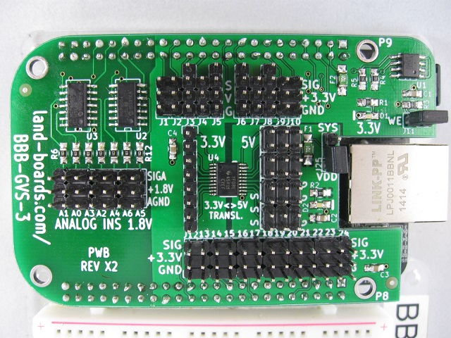
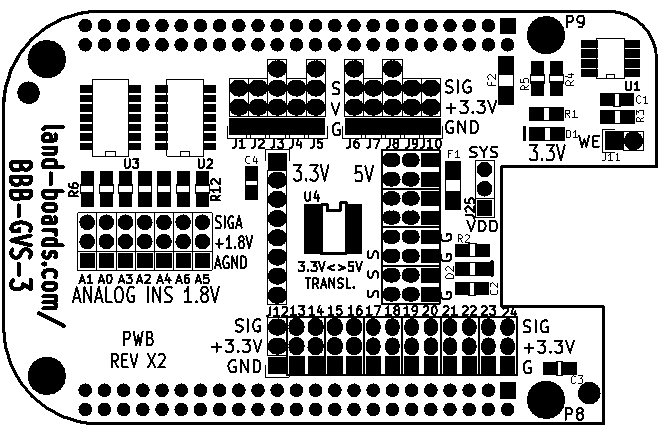
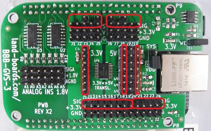
Features
- (19) GPIOs, GVS pins
- GVS pins
- (3) UARTs, GVTxRx pins
- Gnd, Vcc, Tx, Rx pins
- (1) I2C bus, G, V, SDA, SCL
- Ground, Voltage, SDA, SCL
- (8) Channels of 3.3V to 5V level translators
- Use female to female jumpers to route the GPIO lines to the translator channels
- 5V side has GVS pins
- (7) 1.8V analog GVS connections with analog voltage/ground
- Buffer Opamps on the analog inputs
- 5V pins are all ESD protected pins with 15 kV of protection
- Selectable 5V source (SYS_5V or VDD_5V)
- LEDs for 3.3V and 5V power
- Cape configuration EEPROM with write enable jumper
- Beaglebone Black form factor
Connectors
J1 Connector - SPI1_D1
Conn	GPIO		BBB Pin
J1	SPI1_D1		P9_30
J2 Connector - GPIO3_19
Conn	GPIO		BBB Pin
J2	GPIO3_19	P9_27
J3 Connector - UART1
Conn	GPIO		BBB Pin
J3_3	UART1_RX	P9_26
J3_4	UART1_TX	P9_24
J4 Connector - GPIO1_17
Conn	GPIO		BBB Pin
J4	GPIO1_17	P9_23
J5 Connector - UART2
Conn	GPIO		BBB Pin
J5_3	UART2_TX	P9_21
J5_4	UART2_RX	P9_22
J6 Connector - I2C1
Conn	GPIO		BBB Pin
J6_3	I2C1_SDA	P9_18
J6_4	I2C1_SCL	P9_17
J7 Connector - GPIO1_16
Conn	GPIO		BBB Pin
J7	GPIO1_16	P9_15
J8 Connector - UART4
Conn	GPIO		BBB Pin
J8_3	UART4_TX	P9_13
J8_4	UART4_RX	P9_11
J9 Connector - EHRPWM1A
Conn	GPIO		BBB Pin
J9	EHRPWM1A	P9_14
J10 Connector - GPIO1_28
Conn	GPIO		BBB Pin
J10	GPIO1_28	P9_12
J12 Connector - GPIO1_29
Conn	GPIO		BBB Pin
J12	GPIO1_29	P8_26
J13 Connector - EHRPWM2A
Conn	GPIO		BBB Pin
J13	EHRPWM2A	P8_19
J14 Connector - GPIO2_1
Conn	GPIO		BBB Pin
J14	GPIO2_1		P8_18
J15 Connector - GPIO0_27
Conn	GPIO		BBB Pin
J15	GPIO0_27	P8_17
J16 Connector - GPIO1_14
Conn	GPIO		BBB Pin
J16	GPIO1_14	P8_16
J17 Connector - GPIO1_15
Conn	GPIO		BBB Pin
J17	GPIO1_15	P8_15
J18 Connector - EHRPWM2B
Conn	GPIO		BBB Pin
J18	EHRPWM2B	P8_13
J19 Connector - GPIO1_12
Conn	GPIO		BBB Pin
J19	GPIO1_12	P8_12
J20 Connector - GPIO1_13
Conn	GPIO		BBB Pin
J20	GPIO1_13	P8_11
J21 Connector - TIMER5
Conn	GPIO		BBB Pin
J21	TIMER5		P8_09
J22 Connector - TIMER6
Conn	GPIO		BBB Pin
J22	TIMER6		P8_10
J23 Connector - TIMER4
Conn	GPIO		BBB Pin
J23	TIMER4		P8_07
J24 Connector - TIMER7
Conn	GPIO		BBB Pin
J24	TIMER7		P8_08
J25 Connector - 5V Selection Jumper
- 1-2 = SYS_5V
- 2-3 = VDD_5V
VDD_5V is the main power supply from the DC input jack. This voltage is not present when the board is powered via USB. The amount of current supplied by this rail is dependent upon the amount of current available. Based on the board design, this rail is limited to 1A per pin from the main board.
The SYS_5V rail is the main rail for the regulators on the main board. When powered from a DC supply or USB, this rail will be 5V. The available current from this rail depends on the current available from the USB and DC external supplies.
- Available current (per pin)
- 1000mA (x2 pins), VDD_5V
- 250mA (x2 pins), SYS_5V
J11 - Write Enable (WE)
- Install for write enable
- Remove for write protect
EEPROM Connections
- The EEPROM connections are on I2C and have on-board pullup resistors.
- The connections are local to the card.
- The EEPROM part number is CAT24C256WI-GT3
Python pin assignments by header J number
J1 = "P9_30"		# GR-1 - D0
J2 = "P9_27"		# BL-1 - D16
J3_3 = "P9_26"		# VI-1 - D1
J3_4 = "P9_24"		# GY-1 - D17
J4 = "P9_23"		# WH-1 - D2
J5_3 = "P9_21"		# BL-1 - D18
J5_4 = "P9_22"		# BR-2 - D3
J7 = "P9_15"		# RD-2 - D19
J8_3 = "P9_13"		# OR-2 - D4
J8_4 = "P9_11"		# YL-2 - D20
J9 = "P9_14"		# GR-2 - D5
J10 = "P9_12"		# BU-2 - D21
J20 = "P8_11"		# VI-2 - D6
J21 = "P8_9"		# GY-2 - D22
J22 = "P8_10"		# WH-2 - D7
J23 = "P8_7"		# BL-2 - D23
J24 = "P8_8"		# BR-3 - D8
J12 = "P8_26"		# RD-3 - D24
J13 = "P8_19"		# OR-3 - D9
J14 = "P8_18"		# YL-3 - D25
J15 = "P8_17"		# GR-3 - D10
J16 = "P8_16"		# BU-3 - D26
J17 = "P8_15"		# VI-3 - D11
J18 = "P8_13"		# GY-3 - D27
J19 = "P8_12"		# WH-3 - D12
Production Test Procedure
Setup
- Install BBB-GVS-3 on Rev C BeagleBone Black card
- Install shunt at SYS on J25 (5VSEL)
- Install shunt at WE
- Ethernet connection to BBB
- Power via 5V jack to BBB
- Verify 5V and 3.3V LEDs on the card are lit
- BBB are located on the Secondary net at:
- BBB Rev C - 192.168.1.177
- BBB Rev B - 192.168.2.110
- Log in via putty
- User = root
- Password = enter
EEPROM Programming
- Go to directory
- Program the EEPROM
- [mkeeprom code folder
- Verify by typing
cd ~/pyBBB/BBB-GVS-3/mkeeprom
cat data.eeprom > /sys/bus/i2c/devices/1-0054/eeprom
cat /sys/bus/i2c/devices/1-0054/eeprom | hexdump -C
- Result should be like -
00000000  aa 55 33 ee 41 30 42 42  42 2d 47 56 53 2d 33 00  |.U3.A0BBB-GVS-3.|
00000010  00 00 00 00 00 00 00 00  00 00 00 00 00 00 00 00  |................|
00000020  00 00 00 00 00 00 58 31  00 00 4c 61 6e 64 20 42  |......X1..Land B|
00000030  6f 61 72 64 73 2c 20 4c  4c 43 42 42 42 2d 47 56  |oards, LLCBBB-GV|
00000040  53 2d 33 00 00 00 00 00  00 00 00 00 30 30 30 30  |S-3.........0000|
00000050  00 00 00 00 00 00 00 00  00 00 00 00 00 00 00 00  |................|
*
000000e0  00 00 00 00 00 00 00 00  00 00 00 00 00 fa 01 f4  |................|
000000f0  00 fa 00 00 ff ff ff ff  ff ff ff ff ff ff ff ff  |................|
00000100  ff ff ff ff ff ff ff ff  ff ff ff ff ff ff ff ff  |................|
*
00008000
- Remove WE jumper
- Type
cat data.eeprom > /sys/bus/i2c/devices/1-0054/eeprom
- Result should be error
root@BBB01:~/pyBBB/BBB-GVS-3/mkeeprom# cat data.eeprom > /sys/bus/i2c/devices/1-0054/eeprom
cat: write error: Connection timed out
Analog Testing
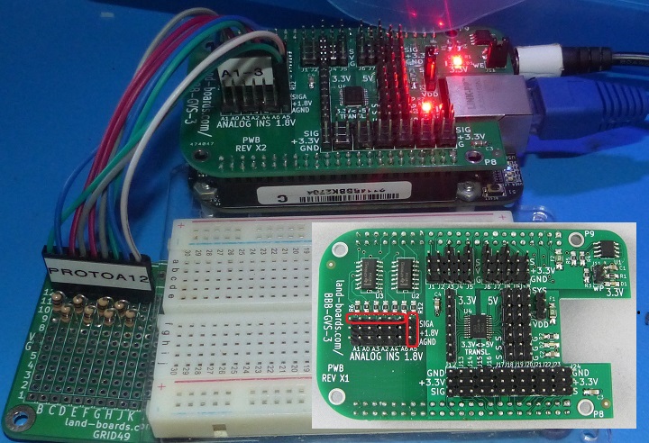
- GRID49 card has a resistor ladder
- (8) 10K resistors
- From 1.8V to all 7 inputs to ground
- Input in 1/8 steps
- Cable connections
- 1x9 end marked "PROTOA12" plugs into resistor card with "PROTOA12" label facing towards resistors
- Green wire at A1 grid location on GRID49 card, white wire at K12 grid location
- 3-pin connector marked "A5" goes to A5
- Label faces Ethernet jack
- Green wire goes to ground, white wire goes to +1.8V
- 1x9 end marked "PROTOA12" plugs into resistor card with "PROTOA12" label facing towards resistors
- Run analog ladder code
- May need to run 2x to get accurate value
- analogLadder.py - Analog Test Code
cd ~/pyBBB/BBB-GVS-3/analogLadder
python analogLadder.py
- Pass/Fail message will be displayed
- Ideal values are
val0  0.625
val1  0.125
val2  0.75
val3  0.24
val4  0.50
val5  0.375
val6  0.875
PASS - Analog values match expected ladder values
GPIO Testing
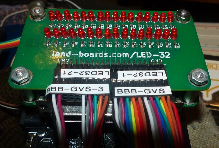
Cable set
- Cables connect LED-32 card in ODAS Test Station to UUT
LED-32 connections
- Hook up LED-32 Card to these pins
BBB-GVS-3 connections
- Connect "loose" 1x8 cable marked "3.3V-SIG" from UUT 3.3V side of translator, connect to "J12-SIG" UUT J12
- Connect 1x8 cable from LED-32 marked "GND" to UUT 5V side of translator GND pins
- Connect 1x8 cable from LED-32 marked "5V-SIG" to UUT 5V side of translator
- Connect 1x5 cable from LED-32 marked "J20-SIG" to UUT J20 SIG pins
- Connect 2x5 cable from LED-32 marked "J1-SIG" to UUT J1
- Connect 2x5 cable from LED-32 marked "J7-SIG" to UUT J6
D0 = "P9_30"		# GR-1 - D0
D1 = "P9_26"		# VI-1 - D1
D2 = "P9_23"		# WH-1 - D2
D3 = "P9_22"		# BR-2 - D3
D4 = "P9_13"		# OR-2 - D4
D5 = "P9_14"		# GR-2 - D5
D6 = "P8_11"		# RD-3 - D6
D7 = "P8_10"		# YL-3 - D7
D8 = "P8_8"		# BU-3 - D8
D9 = "P8_19"		# GY-3 - D9
D10 = "P8_17"		# VI-2 - D10
D11 = "P8_15"		# WH-2 - D11
D12 = "P8_12"		# BR-3 - D12
D27 = "P8_13"		# BL-2 - D27
D26 = "P8_16"		# GY-2 - D26
D25 = "P8_18"		# WH-3 - D25
D24 = "P8_26"		# VI-3 - D24
D23 = "P8_7"		# GR-3 - D23
D22 = "P8_9"		# OR-3 - D22
D21 = "P9_12"		# BU-2 - D21
D20 = "P9_11"		# YL-2 - D20
D19 = "P9_15"		# RD-2 - D19
D18 = "P9_21"		# BL-1 - D18
D17 = "P9_24"		# GY-1 - D17
D16 = "P9_27"		# BL-1 - D16
# Common Ground
Run test
- blink-BBB-GVS-3.py - Test code
cd ~/pyBBB/BBB-GVS-3/blink-BBB-GVS-3/src
python blink-BBB-GVS-3.py
- Lights will circulate around the card in a ring
- CTRL-C to end test
Prepare to re-run
- Type
halt
- Remove 5V Power cable to power of card
Combined Copy/Paste
cd ~/pyBBB/BBB-GVS-3/mkeeprom
cat data.eeprom > /sys/bus/i2c/devices/1-0054/eeprom
cat /sys/bus/i2c/devices/1-0054/eeprom | hexdump -C

cd ~/BBB/BBB-GVS-3/analogLadder
python analogLadder.py

cd ~/pyBBB/BBB-GVS-3/blink-BBB-GVS-3/src
python blink-BBB-GVS-3.py

halt
Drivers / Example Code
Blink LEDs code
I2C Example Code
Issues
Issues with X2 card
- No known or reported issues
Issues with X1 card
- WP jumper should be WE
- EEPROM A3 s/b high not low
- Cut etch to U1-3
- Add wire U1-3 to U1-8

