Difference between revisions of "VGAX49"
Jump to navigation
Jump to search
Blwikiadmin (talk | contribs) |
Blwikiadmin (talk | contribs) |
||
| (12 intermediate revisions by the same user not shown) | |||
| Line 1: | Line 1: | ||
| + | [[File:tindie-mediums.png|link=https://www.tindie.com/products/land_boards/ps2-keyboardmouse-adapter-pcb-only-ps2x49/]] | ||
| + | |||
[[File:VGAX49_P901-cropped-720px.jpg]] | [[File:VGAX49_P901-cropped-720px.jpg]] | ||
== Features == | == Features == | ||
| − | * | + | * Analog VGA adapter |
| − | * 16-bit digital video | + | * Up to 16-bit digital video |
| − | ** 5:6:5 (R:G:B) mapping (maximum) | + | ** 5:6:5 (R:G:B) mapping (maximum- 16 bits) |
| − | ** 2:2:2 (R:G:B) mapping (option) | + | ** 3:3:2 (R:G:B) mapping (option - 8 bits) |
| + | ** 2:2:2 (R:G:B) mapping (option - 6 bits) | ||
| + | ** 1:2:1 (R:G:B) mapping (option - 4 bits) | ||
* Uses summing resistors | * Uses summing resistors | ||
* DB-15F connector | * DB-15F connector | ||
| Line 17: | Line 21: | ||
=== J1 - Digital Connections === | === J1 - Digital Connections === | ||
| + | |||
| + | [[file:VGAX49_J1.PNG]] | ||
| + | |||
| + | * Ex: R0 is the least significant Red bit (connects to 10K resistor) | ||
=== P1 - VGA connector === | === P1 - VGA connector === | ||
| Line 35: | Line 43: | ||
* Too much effort is put into using precision resistors - the human eye is not that picky | * Too much effort is put into using precision resistors - the human eye is not that picky | ||
| − | == VGA - Ideal Drive 2 | + | == VGA - Ideal Drive 2 bit Case == |
* 3.3V driver requires less than 8 mA | * 3.3V driver requires less than 8 mA | ||
| − | ** | + | ** Configure FPGAs output as 3.3V LVTTL and 8mA drive current |
* Ideal case drive current | * Ideal case drive current | ||
* Full scale video = 0.7V | * Full scale video = 0.7V | ||
| Line 59: | Line 67: | ||
[[File:VGA_Sim_2R_Current.PNG]] | [[File:VGA_Sim_2R_Current.PNG]] | ||
| − | === 5:6:5 Resistor Simulation | + | |
| + | == VGA - Ideal Drive 3 bit Case == | ||
| + | |||
| + | * 3.3V driver requires less than 8 mA | ||
| + | ** Configure FPGAs output as 3.3V LVTTL and 8mA drive current | ||
| + | * Ideal case drive current | ||
| + | * Full scale video = 0.7V | ||
| + | * VGA Termination resistor = 75 Ohms | ||
| + | ** 0.7V into 75 Ohms = 9.33 mA | ||
| + | * R-2R values | ||
| + | ** 5% resistor values are 470 ohms, 1K ohms and 2.2K ohms | ||
| + | *** Produces 0.697V | ||
| + | |||
| + | [[file:VideoDAC_3bit_Voltage.PNG]] | ||
| + | |||
| + | == 5:6:5 Resistor Simulation == | ||
* Assumptions | * Assumptions | ||
Latest revision as of 13:43, 14 July 2022
Contents
Features
- Analog VGA adapter
- Up to 16-bit digital video
- 5:6:5 (R:G:B) mapping (maximum- 16 bits)
- 3:3:2 (R:G:B) mapping (option - 8 bits)
- 2:2:2 (R:G:B) mapping (option - 6 bits)
- 1:2:1 (R:G:B) mapping (option - 4 bits)
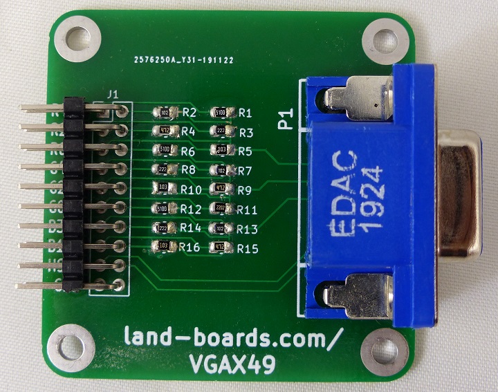
- Uses summing resistors
- DB-15F connector
- 49x49mm ODAS form factor
- Mounting holes
Connectors
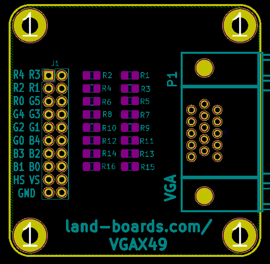
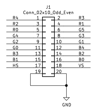
J1 - Digital Connections
- Ex: R0 is the least significant Red bit (connects to 10K resistor)
P1 - VGA connector
Simulation
- Each color is independently driven and can be considered individually
- Critical design criteria is output voltage and current capability of the driving part
- Use common value, 5% resistors
- Each resistor is about 2X the value of the previous resistor
- 1V is drive level for VGA specification
- VGA presents a 75 Ohm load
- 1V at 75 Ohms is 13.3 mA
- Series resistors present a voltage divider between the resistors on the card and the VGA load
- The resistor with the smallest resistance value has larger current from the source device pin
- Current switches from source to sink depending on the voltages on the other resistors
- Each resistor is 2X the value of the previous resistor
- Too much effort is put into using precision resistors - the human eye is not that picky
VGA - Ideal Drive 2 bit Case
- 3.3V driver requires less than 8 mA
- Configure FPGAs output as 3.3V LVTTL and 8mA drive current
- Ideal case drive current
- Full scale video = 0.7V
- VGA Termination resistor = 75 Ohms
- 0.7V into 75 Ohms = 9.33 mA
- R-2R values
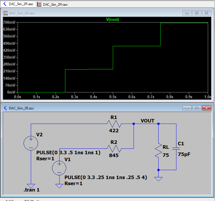
- Ideal resistor values are 417.9 ohms and 835.7 ohms
- Standard value 1% resistors
- 1% standard values are:
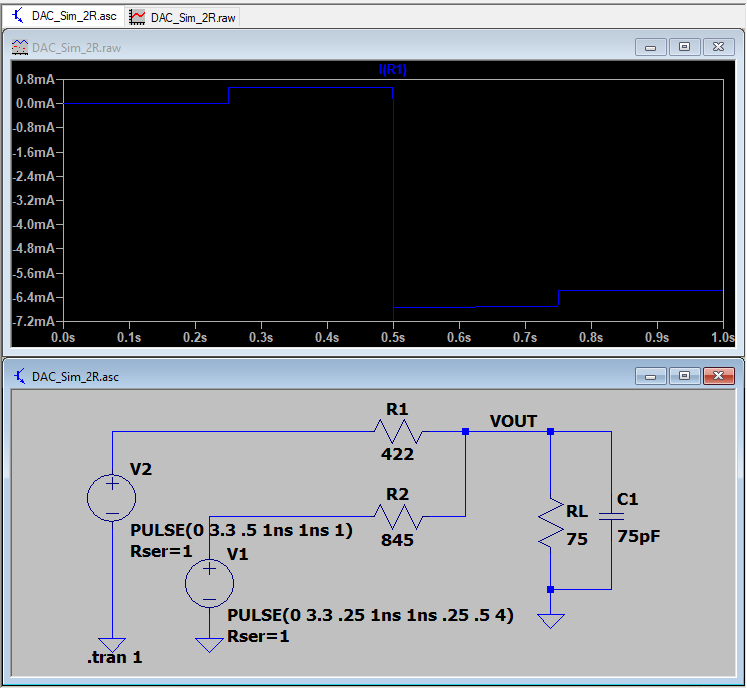
- R1 = 422 (Mouser) Ohms
- R2 = 845 (Mouser) Ohms
- Get closest values
- 0V, 0.228V, 0.460V, 0.693V
- Voltage steps are:
- Current steps are:
VGA - Ideal Drive 3 bit Case
- 3.3V driver requires less than 8 mA
- Configure FPGAs output as 3.3V LVTTL and 8mA drive current
- Ideal case drive current
- Full scale video = 0.7V
- VGA Termination resistor = 75 Ohms
- 0.7V into 75 Ohms = 9.33 mA
- R-2R values
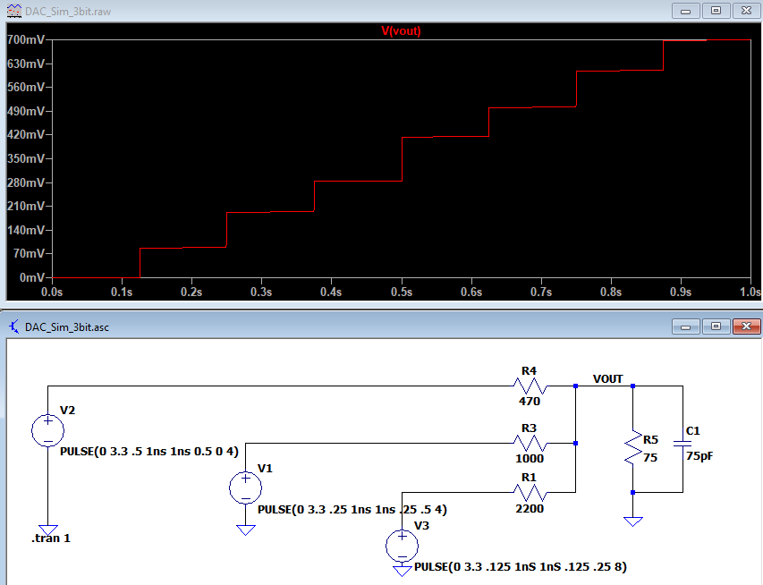
- 5% resistor values are 470 ohms, 1K ohms and 2.2K ohms
- Produces 0.697V
- 5% resistor values are 470 ohms, 1K ohms and 2.2K ohms
5:6:5 Resistor Simulation
- Assumptions
- 3.3V Drive out of FPGA
- 8 mA max drive current (typical FPGA drive current)
- Using common value, 5% resistors
- Model most significant bit resistor as 1/2 the full scale voltage (0.7V) single resistor value
- 75 Ohm terminator in monitor
- 0.7V at 75 Ohms = 9.33mA
- Series resistor - single resistor value is (3.3V-0.7V)/9.33mA is 278.6 Ohms
- First resistor is 2x 278.57 = 557.1 Ohms
- Each resistor is 2x the previous resistor
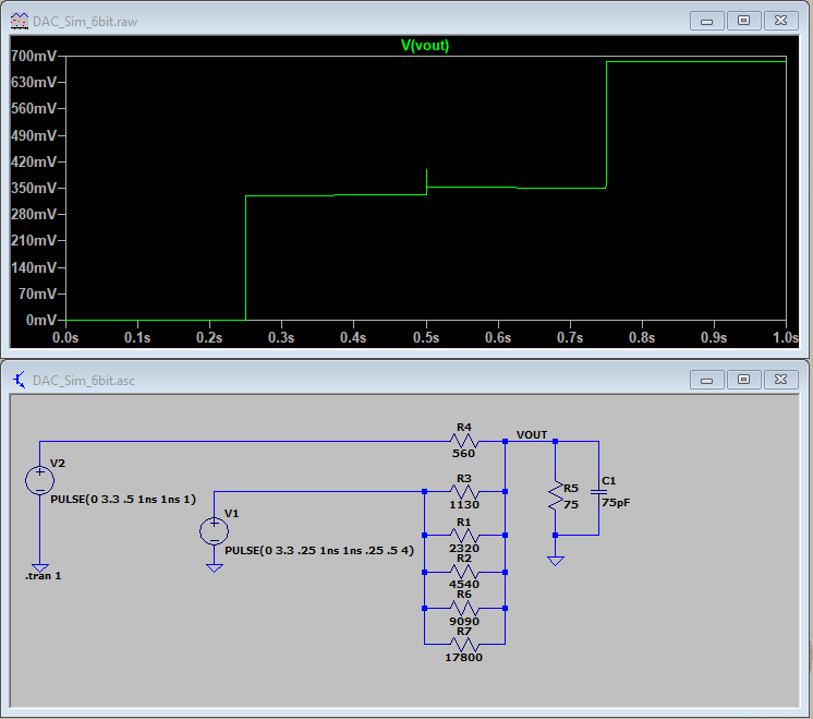
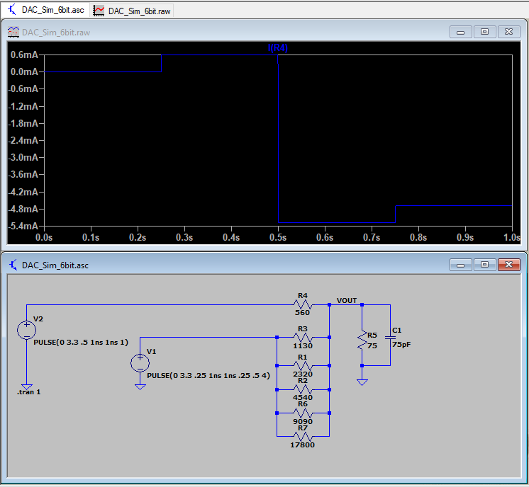
- Simulation uses the same 4 value steps (real case would have 2^5 or 2^6 steps)
- Voltage steps
- Current steps

