Difference between revisions of "TinySA"
Jump to navigation
Jump to search
Blwikiadmin (talk | contribs) |
Blwikiadmin (talk | contribs) |
||
| (18 intermediate revisions by the same user not shown) | |||
| Line 1: | Line 1: | ||
| + | [[file:tinySA.jpg]] | ||
| + | |||
== TinySA - Spectrum Analyzer - Specifications == | == TinySA - Spectrum Analyzer - Specifications == | ||
| Line 84: | Line 86: | ||
* 3.3V at 50 Ohm = 0.2178W | * 3.3V at 50 Ohm = 0.2178W | ||
** 217.8 mW = 23.4 dBm | ** 217.8 mW = 23.4 dBm | ||
| + | |||
| + | == Attenuators == | ||
| + | |||
| + | * [[RF Attenuators|Homebrew RF Attenuators]] | ||
| + | * [[PE4302 RF Attenuator]] - Digitally controlled attenuator | ||
== References == | == References == | ||
* [https://www.tinysa.org/wiki/ tinySA wiki] | * [https://www.tinysa.org/wiki/ tinySA wiki] | ||
| + | * [http://athome.kaashoek.com/tinySA/Windows/ tinySA-App Software] | ||
* [https://store2.rlham.com/shop/catalog/product_info.php?products_id=75243&osCsid=adsqkp0uum898eahocj1marc43 R&L page] | * [https://store2.rlham.com/shop/catalog/product_info.php?products_id=75243&osCsid=adsqkp0uum898eahocj1marc43 R&L page] | ||
| − | |||
| − | |||
| − | |||
| − | |||
| − | |||
| − | |||
| − | |||
| − | |||
| − | |||
| − | |||
| − | |||
| − | |||
| − | |||
| − | |||
| − | |||
| − | |||
| − | |||
| − | |||
| − | |||
| − | |||
| − | |||
| − | |||
| − | |||
| − | |||
| − | |||
| − | |||
| − | |||
| − | |||
| − | |||
| − | |||
| − | |||
| − | |||
| − | |||
| − | |||
| − | |||
| − | |||
| − | |||
| − | |||
| − | |||
| − | |||
| − | |||
| − | |||
| − | |||
| − | |||
| − | |||
| − | |||
| − | |||
| − | |||
| − | |||
| − | |||
| − | |||
| − | |||
| − | |||
| − | |||
| − | |||
| − | |||
| − | |||
| − | |||
== Measurements == | == Measurements == | ||
| Line 156: | Line 106: | ||
[[file:Tiny-SA App v1.1.19.20.PNG]] | [[file:Tiny-SA App v1.1.19.20.PNG]] | ||
| − | === VFO- | + | === VFO-001 === |
| + | |||
| + | [[File:VFO-001_P132-720px.jpg]] | ||
| − | * [[VFO- | + | * [[VFO-001]] |
| − | * 20 MHz | + | * Set to 20 MHz |
* 3.3V square wave drive | * 3.3V square wave drive | ||
* Rich odd harmonic content | * Rich odd harmonic content | ||
| Line 168: | Line 120: | ||
[[file:VFO-002_20dB_001.PNG]] | [[file:VFO-002_20dB_001.PNG]] | ||
| − | === | + | == Attenuator Charts == |
| − | |||
| − | |||
| − | |||
| − | |||
| − | |||
| − | |||
| − | |||
| − | |||
| − | |||
| − | |||
| − | |||
| − | |||
| − | |||
| − | |||
| − | |||
| − | |||
| − | |||
| − | |||
| − | |||
| − | |||
| − | |||
| − | |||
| − | + | [[file:dBm_vs_milliVolt_milliWatts.PNG]] | |
| − | |||
| − | [[file: | + | [[file:dBm_vs_Volta_Watts.PNG]] |
| − | + | [[file:dBm_vs_Volt_Watts.PNG]] | |
| − | |||
| − | |||
| − | + | == Calibrating the Frequency of the tinySA == | |
| − | + | <video type="youtube">5dHFF03mupI</video> | |
== Videos == | == Videos == | ||
| Line 212: | Line 139: | ||
<video type="youtube">qxH0CQOf2NM</video> | <video type="youtube">qxH0CQOf2NM</video> | ||
| + | |||
| + | <video type="youtube">1mulRI-EZ80</video> | ||
Latest revision as of 16:09, 21 August 2022
Contents
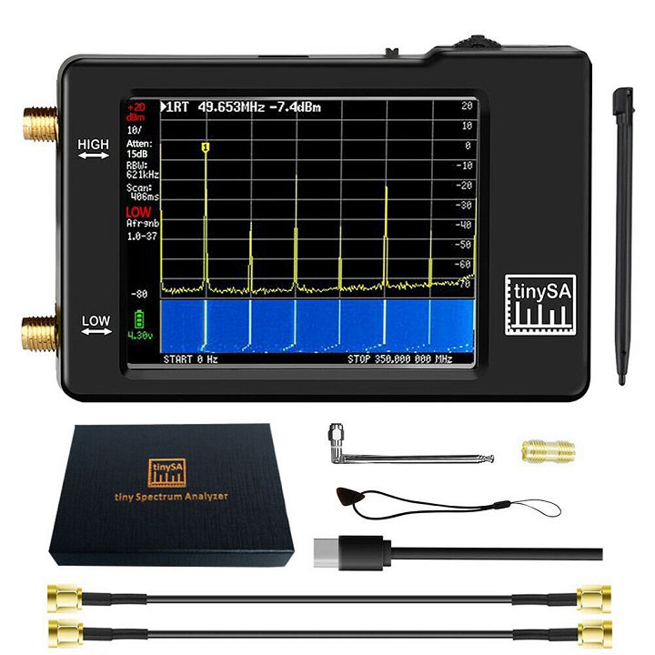
TinySA - Spectrum Analyzer - Specifications
User interface
- Display resolution 320*240 pixels
- Screen diagonal 2.8"
- 16 bits per RGB pixels
- Resistive touch control
- Jog switch control
- USB serial port control
- Optional TTL USART port (SW not yet implemented) on the internal PCB
- Linear power supply to avoid switching noise.
The input/output specification of the tinySA is split over the 4 modes
Low input mode spec
- Input frequency range from 100kHz to 350MHz
- Input impedance 50 ohm when input attenuation set to 10dB or more.
- Selectable manual and automatic input attenuation between 0dB and 31dB in 1 dB steps
- Absolute maximum input level without attenuation of +10dBm
- Absolute maximum input power with 30dB attenuation of +20dBm for short period
- Input Intercept Point of third order modulation products (IIP3) with 0dB attenuation of +15dBm
- 1dB compression point at +2dBm with 0dB attenuation
- Power detector resolution of 0.5dB and linearity versus frequency of +/-1dB
- Absolute power level accuracy after power level calibration of +/- 1dB
- Lowest discernible signal using a resolution bandwidth of 30kHz of -102dBm
- Frequency accuracy equal to the selected resolution bandwidth
- Phase noise of -90dB/Hz at 100kHz offset and -115dB/Hz at 1MHz offset
- Spur free dynamic range when using a 30kHz resolution bandwidth of 70dB
- Manually selectable resolution filters of 3, 10, 30, 100, 300, 600kHz. Automatic selection of one of the 57 resolution filters.
- On screen resolution of 145 or 290 measurement points.
- Scanning speed of over 1000 points/second using largest resolution filters.
- Automatic optimization of actual scanning points to ensure coverage of the whole scan range regardless of the chosen resolution bandwidth
- Spur suppression option for assessing if certain signals are internally generated or actually present in the input signal
High input mode spec
- Input frequency range from 240MHz to 960MHz
- As there is no input bandfilter strong signals outside the 240MHz to 960MHz range can cause distortion of the in band signals
- Absolute maximum input level without attenuation of +10dBm
- Input Intercept Point of third order modulation products (IIP3) of -5dBm
- 1dB compression point at -6dBm with 0dB attenuation
- Power detector resolution of 0.5dB and linearity versus frequency of +/-1dB
- Absolute power level accuracy after power level calibration of +/- 1dB
- Lowest discernible signal using a resolution bandwidth of 30kHz of -115dBm
- Frequency accuracy equal to the selected resolution bandwidth
- Spur free dynamic range when using a 30kHz resolution bandwidth of 50dB
- Selectable (automatic and manual) resolution filters of 3, 10, 30, 100, 300 and 600kHz
- Optional 25dB to 40dB frequency dependent input attenuator. The power level error with this attenuator activated increases to +/- 15dB
- On screen resolution of 145 or 290 measurement points.
- Scanning speed of over 1000 points/second using largest resolution filters.
- Automatic optimization of actual scanning points to ensure coverage of the whole scan range regardless of the chosen resolution bandwidth
Low output mode spec
- Sinus output with harmonics below -40dB of fundamental
- Output frequency range from 100kHz to 350MHz
- Output level selectable in 1dB steps between -76dBm and -6dBm
- Optional AM, narrow FM and wide FM modulation or slow sweep over selectable frequency span
High output mode spec
- Square wave output
- Output frequency range from 240MHz to 960MHz
- Output level selectable in variable increments between -38dBm and +13dBm
- Optional narrow FM and wide FM modulation or slow sweep over selectable frequency span
Reference generator spec
- Optional square wave output with fundamental at -25dBm connected to high input/output
- Frequency can be set to 1MHz, 2MHz, 4MHz, 10MHz, 15MHz or 30MHz.
Battery spec
- Charging time max 1 hour on 500mA minimum USB port or USB charger
- Operation on fully charged battery for at least 2 hours
- Maximum input level
- 0 dBm = 1 mW
- dBm = 10*LOG(milliwatts)
- -10 dBm = 0.1 mW
- +10dBm = 10 mW
- +20dBm = 1000 mW
- 3.3V at 50 Ohm = 0.2178W
- 217.8 mW = 23.4 dBm
Attenuators
- Homebrew RF Attenuators
- PE4302 RF Attenuator - Digitally controlled attenuator
References
Measurements
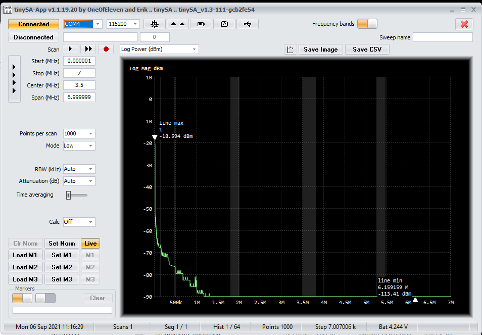
No Stimulus
- 50 Ohm terminator on Low port
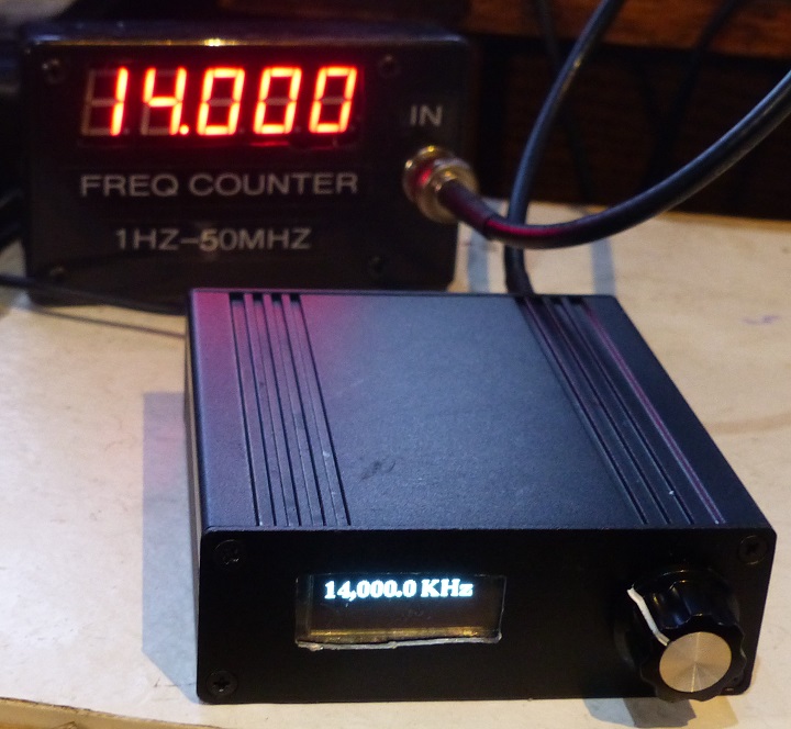
VFO-001
- VFO-001
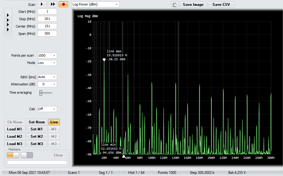
- Set to 20 MHz
- 3.3V square wave drive
- Rich odd harmonic content
- Lots of other noise
- Using 20 dB attenuator (from above)
- 1-301 MHz
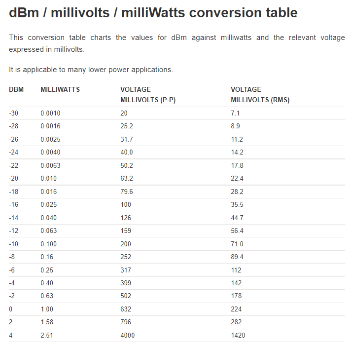
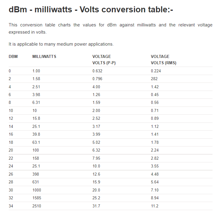
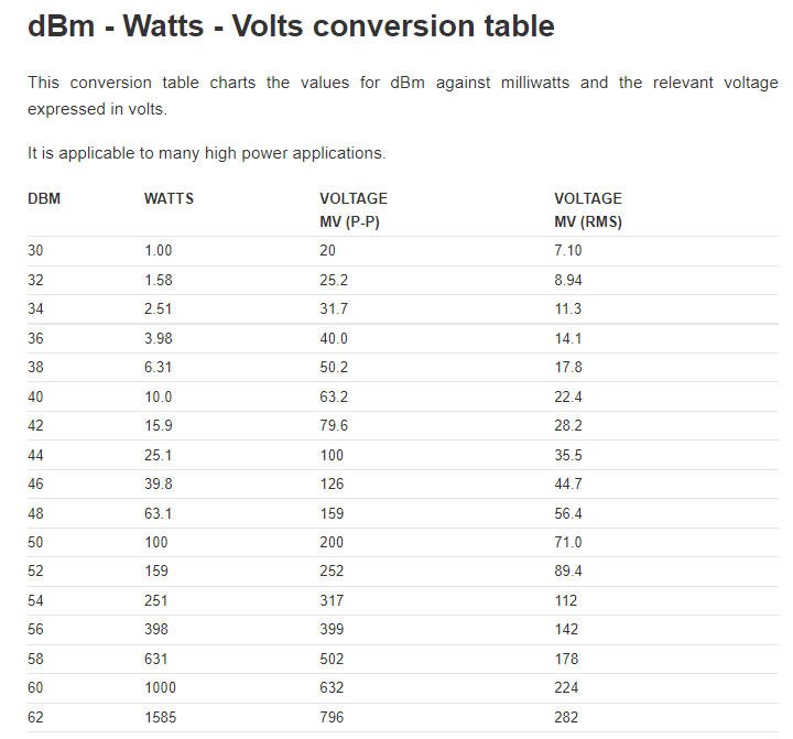
Attenuator Charts
Calibrating the Frequency of the tinySA
Videos
