Difference between revisions of "RETRO-65C816"
Jump to navigation
Jump to search
Blwikiadmin (talk | contribs) |
Blwikiadmin (talk | contribs) |
||
| (36 intermediate revisions by the same user not shown) | |||
| Line 1: | Line 1: | ||
| − | [[file:RETRO- | + | [[RETRO-65C816 Rev 1]] |
| + | |||
| + | [[file:RETRO-65C816_REV2_FRONT.png]] | ||
== Features == | == Features == | ||
| Line 19: | Line 21: | ||
** Tx/Rx LEDs | ** Tx/Rx LEDs | ||
* VGA | * VGA | ||
| − | ** | + | ** 3:3:2 R:G:B |
* PS/2 keyboard | * PS/2 keyboard | ||
** 5V KEYBOARD | ** 5V KEYBOARD | ||
| Line 52: | Line 54: | ||
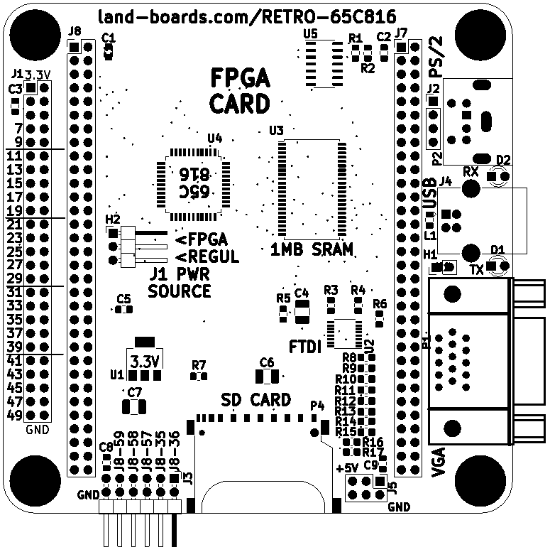
== Connectors == | == Connectors == | ||
| − | [[file:RETRO- | + | [[file:RETRO-65C816_REV2_CAD.PNG]] |
=== H1 - 5V === | === H1 - 5V === | ||
| Line 70: | Line 72: | ||
=== J1 - I/O Connector=== | === J1 - I/O Connector=== | ||
| − | [[FILE:RETRO- | + | [[FILE:RETRO-65C816_REV2_J1_IO.PNG]] |
* 50-pin I/O Connector | * 50-pin I/O Connector | ||
| Line 84: | Line 86: | ||
=== J3 - 6 FPGA pins === | === J3 - 6 FPGA pins === | ||
| − | [[FILE:RETRO- | + | [[FILE:RETRO-65C816_REV2_J3_IO6.PNG]] |
| − | [[FILE:RETRO- | + | [[FILE:RETRO-65C816_REV2_J3_SCHEM_IO6.PNG]] |
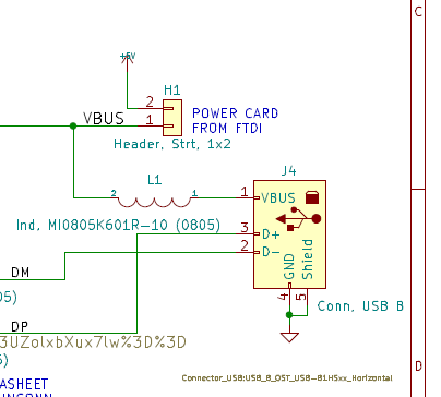
=== J4 - USB B Serial/Power === | === J4 - USB B Serial/Power === | ||
| Line 106: | Line 108: | ||
{| class="wikitable" | {| class="wikitable" | ||
| + | ! U7 PIN | ||
| + | ! EP4CE15 | ||
| + | ! EP4CE55 | ||
| + | ! 5CEFA2 | ||
| + | ! CYC 10 | ||
| + | ! FUNCTION | ||
| + | ! | ||
! U7 PIN | ! U7 PIN | ||
! EP4CE15 | ! EP4CE15 | ||
| Line 119: | Line 128: | ||
| GND | | GND | ||
| GND | | GND | ||
| − | | | + | | |
| 2 | | 2 | ||
| GND | | GND | ||
| Line 133: | Line 142: | ||
| 3.3V | | 3.3V | ||
| 3.3V | | 3.3V | ||
| − | | | + | | |
| 4 | | 4 | ||
| 3.3V | | 3.3V | ||
| Line 147: | Line 156: | ||
| GND | | GND | ||
| GND | | GND | ||
| − | | | + | | |
| 6 | | 6 | ||
| GND | | GND | ||
| Line 161: | Line 170: | ||
| PIN_G1 | | PIN_G1 | ||
| PS2CLK | | PS2CLK | ||
| − | | | + | | |
| 8 | | 8 | ||
| PIN_R2 | | PIN_R2 | ||
| Line 175: | Line 184: | ||
| PIN_D1 | | PIN_D1 | ||
| SRAMA4 | | SRAMA4 | ||
| − | | | + | | |
| 10 | | 10 | ||
| PIN_P2 | | PIN_P2 | ||
| Line 189: | Line 198: | ||
| PIN_B1 | | PIN_B1 | ||
| SRAMA3 | | SRAMA3 | ||
| − | | | + | | |
| 12 | | 12 | ||
| PIN_N2 | | PIN_N2 | ||
| Line 203: | Line 212: | ||
| PIN_D3 | | PIN_D3 | ||
| SRAMA2 | | SRAMA2 | ||
| − | | | + | | |
| 14 | | 14 | ||
| PIN_M2 | | PIN_M2 | ||
| Line 217: | Line 226: | ||
| PIN_B3 | | PIN_B3 | ||
| SRAMA1 | | SRAMA1 | ||
| − | | | + | | |
| 16 | | 16 | ||
| PIN_J2 | | PIN_J2 | ||
| Line 231: | Line 240: | ||
| PIN_B4 | | PIN_B4 | ||
| SRAMA0 | | SRAMA0 | ||
| − | | | + | | |
| 18 | | 18 | ||
| PIN_H2 | | PIN_H2 | ||
| Line 245: | Line 254: | ||
| PIN_E5 | | PIN_E5 | ||
| SRAMCS_N | | SRAMCS_N | ||
| − | | | + | | |
| 20 | | 20 | ||
| PIN_F2 | | PIN_F2 | ||
| Line 259: | Line 268: | ||
| PIN_D4 | | PIN_D4 | ||
| SRAMD0 | | SRAMD0 | ||
| − | | | + | | |
| 22 | | 22 | ||
| PIN_D2 | | PIN_D2 | ||
| Line 273: | Line 282: | ||
| PIN_C6 | | PIN_C6 | ||
| SRAMD1 | | SRAMD1 | ||
| − | | | + | | |
| 24 | | 24 | ||
| PIN_C2 | | PIN_C2 | ||
| Line 287: | Line 296: | ||
| PIN_B5 | | PIN_B5 | ||
| SRAMD2 | | SRAMD2 | ||
| − | | | + | | |
| 26 | | 26 | ||
| − | | | + | | PIN_B2 |
| − | | | + | | PIN_B2 |
| PIN_H8 | | PIN_H8 | ||
| PIN_A5 | | PIN_A5 | ||
| Line 296: | Line 305: | ||
|- | |- | ||
| 27 | | 27 | ||
| − | | | + | | PIN_B3 |
| − | | | + | | PIN_B3 |
| PIN_F7 | | PIN_F7 | ||
| PIN_B6 | | PIN_B6 | ||
| SRAMD3 | | SRAMD3 | ||
| − | | | + | | |
| 28 | | 28 | ||
| − | | | + | | PIN_A3 |
| − | | | + | | PIN_A3 |
| PIN_E7 | | PIN_E7 | ||
| PIN_A6 | | PIN_A6 | ||
| Line 310: | Line 319: | ||
|- | |- | ||
| 29 | | 29 | ||
| − | | | + | | PIN_B4 |
| − | | | + | | PIN_B4 |
| PIN_D6 | | PIN_D6 | ||
| PIN_B7 | | PIN_B7 | ||
| SRAMWE_N | | SRAMWE_N | ||
| − | | | + | | |
| 30 | | 30 | ||
| − | | | + | | PIN_A4 |
| − | | | + | | PIN_A4 |
| PIN_C6 | | PIN_C6 | ||
| PIN_A7 | | PIN_A7 | ||
| Line 324: | Line 333: | ||
|- | |- | ||
| 31 | | 31 | ||
| − | | | + | | PIN_C4 |
| − | | | + | | PIN_C4 |
| PIN_E9 | | PIN_E9 | ||
| PIN_D8 | | PIN_D8 | ||
| SRAMA19 | | SRAMA19 | ||
| − | | | + | | |
| 32 | | 32 | ||
| − | | | + | | PIN_C3 |
| − | | | + | | PIN_C3 |
| PIN_D9 | | PIN_D9 | ||
| PIN_C8 | | PIN_C8 | ||
| Line 338: | Line 347: | ||
|- | |- | ||
| 33 | | 33 | ||
| − | | | + | | PIN_B5 |
| − | | | + | | PIN_B5 |
| PIN_B5 | | PIN_B5 | ||
| PIN_D9 | | PIN_D9 | ||
| SRAMA18 | | SRAMA18 | ||
| − | | | + | | |
| 34 | | 34 | ||
| − | | | + | | PIN_A5 |
| − | | | + | | PIN_A5 |
| PIN_A5 | | PIN_A5 | ||
| PIN_C9 | | PIN_C9 | ||
| Line 352: | Line 361: | ||
|- | |- | ||
| 35 | | 35 | ||
| − | | | + | | PIN_B6 |
| − | | | + | | PIN_B6 |
| PIN_B6 | | PIN_B6 | ||
| PIN_B8 | | PIN_B8 | ||
| SRAMA17 | | SRAMA17 | ||
| − | | | + | | |
| 36 | | 36 | ||
| − | | | + | | PIN_A6 |
| − | | | + | | PIN_A6 |
| PIN_B7 | | PIN_B7 | ||
| PIN_A8 | | PIN_A8 | ||
| Line 366: | Line 375: | ||
|- | |- | ||
| 37 | | 37 | ||
| − | | | + | | PIN_B7 |
| − | | | + | | PIN_B7 |
| PIN_A7 | | PIN_A7 | ||
| PIN_B9 | | PIN_B9 | ||
| SRAMA16 | | SRAMA16 | ||
| − | | | + | | |
| 38 | | 38 | ||
| − | | | + | | PIN_A7 |
| − | | | + | | PIN_A7 |
| PIN_A8 | | PIN_A8 | ||
| PIN_A9 | | PIN_A9 | ||
| Line 380: | Line 389: | ||
|- | |- | ||
| 39 | | 39 | ||
| − | | | + | | PIN_B8 |
| − | | | + | | PIN_B8 |
| PIN_A9 | | PIN_A9 | ||
| PIN_E9 | | PIN_E9 | ||
| N/C | | N/C | ||
| − | | | + | | |
| 40 | | 40 | ||
| − | | | + | | PIN_A8 |
| − | | | + | | PIN_A8 |
| PIN_A10 | | PIN_A10 | ||
| PIN_E8 | | PIN_E8 | ||
| Line 394: | Line 403: | ||
|- | |- | ||
| 41 | | 41 | ||
| − | | | + | | PIN_B9 |
| − | | | + | | PIN_B9 |
| PIN_B10 | | PIN_B10 | ||
| PIN_E11 | | PIN_E11 | ||
| − | | | + | | CARDDET |
| − | | | + | | |
| 42 | | 42 | ||
| − | | | + | | PIN_A9 |
| − | | | + | | PIN_A9 |
| PIN_C9 | | PIN_C9 | ||
| PIN_E10 | | PIN_E10 | ||
| Line 408: | Line 417: | ||
|- | |- | ||
| 43 | | 43 | ||
| − | | | + | | PIN_B10 |
| − | | | + | | PIN_B10 |
| PIN_G10 | | PIN_G10 | ||
| PIN_A10 | | PIN_A10 | ||
| − | | USBRX/ | + | | USBRX/o_FPGATX |
| − | | | + | | |
| 44 | | 44 | ||
| − | | | + | | PIN_A10 |
| − | | | + | | PIN_A10 |
| PIN_F10 | | PIN_F10 | ||
| PIN_B10 | | PIN_B10 | ||
| − | | USBCTS/ | + | | USBCTS/o_FPGARTS |
|- | |- | ||
| 45 | | 45 | ||
| − | | | + | | PIN_B13 |
| − | | | + | | PIN_B13 |
| PIN_C11 | | PIN_C11 | ||
| PIN_D12 | | PIN_D12 | ||
| − | | USBTX/ | + | | USBTX/i_FPGARX |
| − | | | + | | |
| 46 | | 46 | ||
| − | | | + | | PIN_A13 |
| − | | | + | | PIN_A13 |
| PIN_B11 | | PIN_B11 | ||
| PIN_D11 | | PIN_D11 | ||
| − | | UBSRTS/ | + | | UBSRTS/i_FPGACTS |
|- | |- | ||
| 47 | | 47 | ||
| − | | | + | | PIN_B14 |
| − | | | + | | PIN_B14 |
| PIN_B12 | | PIN_B12 | ||
| PIN_B11 | | PIN_B11 | ||
| − | | | + | | REDHI |
| − | | | + | | |
| 48 | | 48 | ||
| − | | | + | | PIN_A14 |
| − | | | + | | PIN_A14 |
| PIN_A12 | | PIN_A12 | ||
| PIN_A11 | | PIN_A11 | ||
| − | | | + | | REDMID |
|- | |- | ||
| 49 | | 49 | ||
| − | | | + | | PIN_B15 |
| − | | | + | | PIN_B15 |
| PIN_E12 | | PIN_E12 | ||
| PIN_B12 | | PIN_B12 | ||
| REDLO | | REDLO | ||
| − | | | + | | |
| 50 | | 50 | ||
| − | | | + | | PIN_A15 |
| − | | | + | | PIN_A15 |
| PIN_D12 | | PIN_D12 | ||
| PIN_A12 | | PIN_A12 | ||
| − | | | + | | GRNHI |
|- | |- | ||
| 51 | | 51 | ||
| − | | | + | | PIN_B16 |
| − | | | + | | PIN_B16 |
| PIN_D13 | | PIN_D13 | ||
| PIN_B13 | | PIN_B13 | ||
| − | | | + | | GRNMID |
| − | | | + | | |
| 52 | | 52 | ||
| − | | | + | | PIN_A16 |
| − | | | + | | PIN_A16 |
| PIN_C13 | | PIN_C13 | ||
| PIN_A13 | | PIN_A13 | ||
| − | | | + | | GRNLO |
|- | |- | ||
| 53 | | 53 | ||
| − | | | + | | PIN_B17 |
| − | | | + | | PIN_B17 |
| PIN_B13 | | PIN_B13 | ||
| PIN_B14 | | PIN_B14 | ||
| − | | | + | | BLUHI |
| − | | | + | | |
| 54 | | 54 | ||
| − | | | + | | PIN_A17 |
| − | | | + | | PIN_A17 |
| PIN_A13 | | PIN_A13 | ||
| PIN_A14 | | PIN_A14 | ||
| − | | | + | | BLULO |
|- | |- | ||
| 55 | | 55 | ||
| − | | | + | | PIN_B18 |
| − | | | + | | PIN_B18 |
| PIN_A15 | | PIN_A15 | ||
| PIN_D14 | | PIN_D14 | ||
| HSYNC | | HSYNC | ||
| − | | | + | | |
| 56 | | 56 | ||
| − | | | + | | PIN_A18 |
| − | | | + | | PIN_A18 |
| PIN_A14 | | PIN_A14 | ||
| PIN_C14 | | PIN_C14 | ||
| Line 506: | Line 515: | ||
|- | |- | ||
| 57 | | 57 | ||
| − | | | + | | PIN_B19 |
| − | | | + | | PIN_B19 |
| PIN_B15 | | PIN_B15 | ||
| PIN_B16 | | PIN_B16 | ||
| SDCS_N | | SDCS_N | ||
| − | | | + | | |
| 58 | | 58 | ||
| − | | | + | | PIN_A19 |
| − | | | + | | PIN_A19 |
| PIN_C15 | | PIN_C15 | ||
| PIN_A15 | | PIN_A15 | ||
| Line 520: | Line 529: | ||
|- | |- | ||
| 59 | | 59 | ||
| − | | | + | | PIN_B20 |
| − | | | + | | PIN_B20 |
| PIN_C16 | | PIN_C16 | ||
| PIN_C16 | | PIN_C16 | ||
| SD_SCK | | SD_SCK | ||
| − | | | + | | |
| 60 | | 60 | ||
| − | | | + | | PIN_A20 |
| − | | | + | | PIN_A20 |
| PIN_B16 | | PIN_B16 | ||
| PIN_C15 | | PIN_C15 | ||
| Line 539: | Line 548: | ||
| GND | | GND | ||
| GND | | GND | ||
| − | | | + | | |
| 62 | | 62 | ||
| GND | | GND | ||
| Line 553: | Line 562: | ||
| VIN | | VIN | ||
| VIN | | VIN | ||
| − | | | + | | |
| 64 | | 64 | ||
| VIN | | VIN | ||
| Line 564: | Line 573: | ||
=== J8 Pin Mapping Card to FPGA pins - Left connector === | === J8 Pin Mapping Card to FPGA pins - Left connector === | ||
| + | |||
| + | * [[QMTECH_Cyclone_10CL006_FPGA_Card#U8 Cyclone 10|Cyclone 10]] notes | ||
| + | ** Cannot place output or bidirectional pin J8IO[35] in input pin location M16 | ||
| + | ** Cannot place output or bidirectional pin J8IO[36] in input pin location M15 | ||
| + | ** Cannot place output or bidirectional pin J8IO[57] in input pin location E16 | ||
| + | ** Cannot place output or bidirectional pin J8IO[58] in input pin location E15 | ||
{| class="wikitable" | {| class="wikitable" | ||
| Line 571: | Line 586: | ||
! 5CEFA2 | ! 5CEFA2 | ||
! 10C1006 | ! 10C1006 | ||
| + | ! J1 | ||
| + | ! Function | ||
| + | ! | ||
| + | ! U8 PIN | ||
| + | ! EP4CE15 | ||
| + | ! EP4CE55 | ||
| + | ! 5CEFA2 | ||
| + | ! 10C1006 | ||
| + | ! J1 | ||
! Function | ! Function | ||
|- | |- | ||
| Line 578: | Line 602: | ||
| GND | | GND | ||
| GND | | GND | ||
| − | | | + | | N/C |
| − | | | + | | |
| + | | | ||
| 2 | | 2 | ||
| GND | | GND | ||
| Line 585: | Line 610: | ||
| GND | | GND | ||
| GND | | GND | ||
| − | | | + | | N/C |
| + | | | ||
|- | |- | ||
| 3 | | 3 | ||
| Line 593: | Line 619: | ||
| 3.3V | | 3.3V | ||
| J1-1 | | J1-1 | ||
| − | | | + | | |
| + | | | ||
| 4 | | 4 | ||
| 3.3V | | 3.3V | ||
| Line 600: | Line 627: | ||
| 3.3V | | 3.3V | ||
| J1-2 | | J1-2 | ||
| + | | | ||
|- | |- | ||
| 5 | | 5 | ||
| Line 606: | Line 634: | ||
| GND | | GND | ||
| GND | | GND | ||
| − | | | + | | N/C |
| − | | | + | | |
| + | | | ||
| 6 | | 6 | ||
| GND | | GND | ||
| Line 613: | Line 642: | ||
| GND | | GND | ||
| GND | | GND | ||
| − | | | + | | N/C |
| + | | | ||
|- | |- | ||
| 7 | | 7 | ||
| Line 620: | Line 650: | ||
| PIN_AA14 | | PIN_AA14 | ||
| PIN_R9 | | PIN_R9 | ||
| + | | N/C | ||
| CPUE | | CPUE | ||
| − | | | + | | |
| 8 | | 8 | ||
| PIN_AB13 | | PIN_AB13 | ||
| Line 627: | Line 658: | ||
| PIN_AA13 | | PIN_AA13 | ||
| PIN_T9 | | PIN_T9 | ||
| + | | N/C | ||
| CPURES* | | CPURES* | ||
|- | |- | ||
| Line 634: | Line 666: | ||
| PIN_AA15 | | PIN_AA15 | ||
| PIN_R10 | | PIN_R10 | ||
| + | | J1-4 | ||
| CPUMX | | CPUMX | ||
| − | | | + | | |
| 10 | | 10 | ||
| PIN_AB14 | | PIN_AB14 | ||
| Line 641: | Line 674: | ||
| PIN_AB15 | | PIN_AB15 | ||
| PIN_T10 | | PIN_T10 | ||
| + | | J1-3 | ||
| CPUCLK | | CPUCLK | ||
|- | |- | ||
| Line 648: | Line 682: | ||
| PIN_Y15 | | PIN_Y15 | ||
| PIN_R11 | | PIN_R11 | ||
| + | | J1-6 | ||
| CPUBE | | CPUBE | ||
| − | | | + | | |
| 12 | | 12 | ||
| PIN_AB15 | | PIN_AB15 | ||
| Line 655: | Line 690: | ||
| PIN_Y13 | | PIN_Y13 | ||
| PIN_T11 | | PIN_T11 | ||
| + | | J1-5 | ||
| CPUNMIB | | CPUNMIB | ||
|- | |- | ||
| Line 662: | Line 698: | ||
| PIN_AB18 | | PIN_AB18 | ||
| PIN_R12 | | PIN_R12 | ||
| + | | J1-8 | ||
| CPURWB | | CPURWB | ||
| − | | | + | | |
| 14 | | 14 | ||
| PIN_AB16 | | PIN_AB16 | ||
| Line 669: | Line 706: | ||
| PIN_AB17 | | PIN_AB17 | ||
| PIN_T12 | | PIN_T12 | ||
| + | | J1-7 | ||
| CPUIRQB | | CPUIRQB | ||
|- | |- | ||
| Line 676: | Line 714: | ||
| PIN_Y7 | | PIN_Y7 | ||
| PIN_N9 | | PIN_N9 | ||
| + | | J1-10 | ||
| CPUVDA | | CPUVDA | ||
| − | | | + | | |
| 16 | | 16 | ||
| PIN_AB17 | | PIN_AB17 | ||
| Line 683: | Line 722: | ||
| PIN_Y16 | | PIN_Y16 | ||
| PIN_M9 | | PIN_M9 | ||
| + | | J1-9 | ||
| CPUABORTB | | CPUABORTB | ||
|- | |- | ||
| Line 690: | Line 730: | ||
| PIN_AA18 | | PIN_AA18 | ||
| PIN_M10 | | PIN_M10 | ||
| + | | J1-12 | ||
| CPUVPA | | CPUVPA | ||
| − | | | + | | |
| 18 | | 18 | ||
| PIN_AB18 | | PIN_AB18 | ||
| Line 697: | Line 738: | ||
| PIN_AA17 | | PIN_AA17 | ||
| PIN_P9 | | PIN_P9 | ||
| + | | J1-11 | ||
| CPURDY | | CPURDY | ||
|- | |- | ||
| Line 704: | Line 746: | ||
| PIN_AA20 | | PIN_AA20 | ||
| PIN_P11 | | PIN_P11 | ||
| + | | J1-14 | ||
| CPUVPB | | CPUVPB | ||
| − | | | + | | |
| 20 | | 20 | ||
| PIN_AB19 | | PIN_AB19 | ||
| Line 711: | Line 754: | ||
| PIN_AA19 | | PIN_AA19 | ||
| PIN_N11 | | PIN_N11 | ||
| + | | J1-13 | ||
| CPUMLB | | CPUMLB | ||
|- | |- | ||
| Line 718: | Line 762: | ||
| PIN_Y20 | | PIN_Y20 | ||
| PIN_R13 | | PIN_R13 | ||
| − | | 16 | + | | I1-16 |
| − | | | + | | |
| + | | | ||
| 22 | | 22 | ||
| PIN_AB20 | | PIN_AB20 | ||
| Line 725: | Line 770: | ||
| PIN_Y19 | | PIN_Y19 | ||
| PIN_T13 | | PIN_T13 | ||
| − | | 15 | + | | J1-15 |
| + | | | ||
|- | |- | ||
| 23 | | 23 | ||
| Line 732: | Line 778: | ||
| PIN_AB21 | | PIN_AB21 | ||
| PIN_T15 | | PIN_T15 | ||
| − | | 18 | + | | J1-18 |
| − | | | + | | |
| + | | | ||
| 24 | | 24 | ||
| PIN_Y21 | | PIN_Y21 | ||
| Line 739: | Line 786: | ||
| PIN_AB20 | | PIN_AB20 | ||
| PIN_T14 | | PIN_T14 | ||
| − | | 17 | + | | J1-17 |
| + | | | ||
|- | |- | ||
| 25 | | 25 | ||
| Line 746: | Line 794: | ||
| PIN_AA22 | | PIN_AA22 | ||
| PIN_N12 | | PIN_N12 | ||
| − | | 20 | + | | J1-20 |
| − | | | + | | |
| + | | | ||
| 26 | | 26 | ||
| PIN_W21 | | PIN_W21 | ||
| Line 753: | Line 802: | ||
| PIN_AB22 | | PIN_AB22 | ||
| PIN_M11 | | PIN_M11 | ||
| − | | 19 | + | | J1-19 |
| + | | | ||
|- | |- | ||
| 27 | | 27 | ||
| Line 760: | Line 810: | ||
| PIN_W22 | | PIN_W22 | ||
| PIN_R14 | | PIN_R14 | ||
| − | | 22 | + | | J1-22 |
| − | | | + | | |
| + | | | ||
| 28 | | 28 | ||
| PIN_V21 | | PIN_V21 | ||
| Line 767: | Line 818: | ||
| PIN_Y22 | | PIN_Y22 | ||
| PIN_N13 | | PIN_N13 | ||
| − | | 21 | + | | J1-21 |
| + | | | ||
|- | |- | ||
| 29 | | 29 | ||
| Line 774: | Line 826: | ||
| PIN_Y21 | | PIN_Y21 | ||
| PIN_N14 | | PIN_N14 | ||
| − | | 24 | + | | J1-24 |
| − | | | + | | |
| + | | | ||
| 30 | | 30 | ||
| PIN_U21 | | PIN_U21 | ||
| Line 781: | Line 834: | ||
| PIN_W21 | | PIN_W21 | ||
| PIN_P14 | | PIN_P14 | ||
| − | | 23 | + | | J1-23 |
| + | | | ||
|- | |- | ||
| 31 | | 31 | ||
| Line 788: | Line 842: | ||
| PIN_U22 | | PIN_U22 | ||
| PIN_P16 | | PIN_P16 | ||
| − | | 26 | + | | J1-26 |
| − | | | + | | |
| + | | | ||
| 32 | | 32 | ||
| PIN_R21 | | PIN_R21 | ||
| Line 795: | Line 850: | ||
| PIN_V21 | | PIN_V21 | ||
| PIN_R16 | | PIN_R16 | ||
| − | | 25 | + | | J1-25 |
| + | | | ||
|- | |- | ||
| 33 | | 33 | ||
| Line 802: | Line 858: | ||
| PIN_V20 | | PIN_V20 | ||
| PIN_N16 | | PIN_N16 | ||
| − | | 28 | + | | J1-28 |
| − | | | + | | |
| + | | | ||
| 34 | | 34 | ||
| PIN_P21 | | PIN_P21 | ||
| Line 809: | Line 866: | ||
| PIN_W19 | | PIN_W19 | ||
| PIN_N15 | | PIN_N15 | ||
| − | | 27 | + | | J1-27 |
| + | | | ||
|- | |- | ||
| 35 | | 35 | ||
| Line 815: | Line 873: | ||
| PIN_N22 | | PIN_N22 | ||
| PIN_U21 | | PIN_U21 | ||
| − | | PIN_M16 | + | | PIN_M16 (Note) |
| − | | | + | | J3-3 |
| − | | | + | | |
| + | | | ||
| 36 | | 36 | ||
| PIN_N21 | | PIN_N21 | ||
| PIN_N21 | | PIN_N21 | ||
| PIN_U20 | | PIN_U20 | ||
| − | | PIN_M15 | + | | PIN_M15 (Note) |
| − | | | + | | J3-1 |
| + | | | ||
|- | |- | ||
| 37 | | 37 | ||
| Line 830: | Line 890: | ||
| PIN_R22 | | PIN_R22 | ||
| PIN_L16 | | PIN_L16 | ||
| − | | | + | | J1-30 |
| − | | | + | | |
| + | | | ||
| 38 | | 38 | ||
| PIN_M21 | | PIN_M21 | ||
| Line 837: | Line 898: | ||
| PIN_T22 | | PIN_T22 | ||
| PIN_L15 | | PIN_L15 | ||
| − | | | + | | J1-29 |
| + | | | ||
|- | |- | ||
| 39 | | 39 | ||
| Line 844: | Line 906: | ||
| PIN_P22 | | PIN_P22 | ||
| PIN_P15 | | PIN_P15 | ||
| − | | | + | | J1-32 |
| − | | | + | | |
| + | | | ||
| 40 | | 40 | ||
| PIN_L21 | | PIN_L21 | ||
| Line 851: | Line 914: | ||
| PIN_R21 | | PIN_R21 | ||
| PIN_M12 | | PIN_M12 | ||
| − | | | + | | J1-31 |
| + | | | ||
|- | |- | ||
| 41 | | 41 | ||
| Line 858: | Line 922: | ||
| PIN_T20 | | PIN_T20 | ||
| PIN_L14 | | PIN_L14 | ||
| − | | | + | | J1-34 |
| − | | | + | | |
| + | | | ||
| 42 | | 42 | ||
| PIN_K21 | | PIN_K21 | ||
| Line 865: | Line 930: | ||
| PIN_T19 | | PIN_T19 | ||
| PIN_L13 | | PIN_L13 | ||
| − | | | + | | J1-33 |
| + | | | ||
|- | |- | ||
| 43 | | 43 | ||
| Line 872: | Line 938: | ||
| PIN_P16 | | PIN_P16 | ||
| PIN_K16 | | PIN_K16 | ||
| − | | | + | | J1-36 |
| − | | | + | | |
| + | | | ||
| 44 | | 44 | ||
| PIN_J21 | | PIN_J21 | ||
| Line 879: | Line 946: | ||
| PIN_P17 | | PIN_P17 | ||
| PIN_K15 | | PIN_K15 | ||
| − | | | + | | J1-35 |
| + | | | ||
|- | |- | ||
| 45 | | 45 | ||
| Line 886: | Line 954: | ||
| PIN_N20 | | PIN_N20 | ||
| PIN_K12 | | PIN_K12 | ||
| − | | | + | | J1-38 |
| − | | | + | | |
| + | | | ||
| 46 | | 46 | ||
| PIN_H21 | | PIN_H21 | ||
| Line 893: | Line 962: | ||
| PIN_N21 | | PIN_N21 | ||
| PIN_J12 | | PIN_J12 | ||
| − | | | + | | J1-37 |
| + | | | ||
|- | |- | ||
| 47 | | 47 | ||
| Line 900: | Line 970: | ||
| PIN_M21 | | PIN_M21 | ||
| PIN_J14 | | PIN_J14 | ||
| − | | | + | | J1-40 |
| − | | | + | | |
| + | | | ||
| 48 | | 48 | ||
| PIN_F21 | | PIN_F21 | ||
| Line 907: | Line 978: | ||
| PIN_M20 | | PIN_M20 | ||
| PIN_J13 | | PIN_J13 | ||
| − | | | + | | J1-39 |
| + | | | ||
|- | |- | ||
| 49 | | 49 | ||
| Line 914: | Line 986: | ||
| PIN_M18 | | PIN_M18 | ||
| PIN_K11 | | PIN_K11 | ||
| − | | | + | | J1-42 |
| − | | | + | | |
| + | | | ||
| 50 | | 50 | ||
| PIN_E21 | | PIN_E21 | ||
| Line 921: | Line 994: | ||
| PIN_N19 | | PIN_N19 | ||
| PIN_J11 | | PIN_J11 | ||
| − | | | + | | J1-41 |
| + | | | ||
|- | |- | ||
| 51 | | 51 | ||
| Line 928: | Line 1,002: | ||
| PIN_L18 | | PIN_L18 | ||
| PIN_G11 | | PIN_G11 | ||
| − | | | + | | J1-44 |
| − | | | + | | |
| + | | | ||
| 52 | | 52 | ||
| PIN_D21 | | PIN_D21 | ||
| Line 935: | Line 1,010: | ||
| PIN_L19 | | PIN_L19 | ||
| PIN_F11 | | PIN_F11 | ||
| − | | | + | | J1-43 |
| + | | | ||
|- | |- | ||
| 53 | | 53 | ||
| Line 942: | Line 1,018: | ||
| PIN_M22 | | PIN_M22 | ||
| PIN_F13 | | PIN_F13 | ||
| − | | | + | | J1-46 |
| − | | | + | | |
| + | | | ||
| 54 | | 54 | ||
| PIN_C21 | | PIN_C21 | ||
| Line 949: | Line 1,026: | ||
| PIN_L22 | | PIN_L22 | ||
| PIN_F14 | | PIN_F14 | ||
| − | | | + | | J1-45 |
| + | | | ||
|- | |- | ||
| 55 | | 55 | ||
| Line 956: | Line 1,034: | ||
| PIN_L17 | | PIN_L17 | ||
| PIN_F10 | | PIN_F10 | ||
| + | | J1-48 | ||
| + | | | ||
| | | | ||
| − | |||
| 56 | | 56 | ||
| PIN_B21 | | PIN_B21 | ||
| Line 963: | Line 1,042: | ||
| PIN_K17 | | PIN_K17 | ||
| PIN_F9 | | PIN_F9 | ||
| + | | J1-47 | ||
| | | | ||
|- | |- | ||
| Line 969: | Line 1,049: | ||
| PIN_N20 | | PIN_N20 | ||
| PIN_K22 | | PIN_K22 | ||
| − | | PIN_E16 | + | | PIN_E16 (Note) |
| + | | J3-5 | ||
| + | | | ||
| | | | ||
| − | |||
| 58 | | 58 | ||
| PIN_N19 | | PIN_N19 | ||
| PIN_N19 | | PIN_N19 | ||
| PIN_K21 | | PIN_K21 | ||
| − | | PIN_E15 | + | | PIN_E15 (Note) |
| + | | J3-7 | ||
| | | | ||
|- | |- | ||
| Line 984: | Line 1,066: | ||
| PIN_M16 | | PIN_M16 | ||
| PIN_D16 | | PIN_D16 | ||
| + | | J3-9 | ||
| + | | | ||
| | | | ||
| − | |||
| 60 | | 60 | ||
| PIN_M19 | | PIN_M19 | ||
| Line 991: | Line 1,074: | ||
| PIN_N16 | | PIN_N16 | ||
| PIN_D15 | | PIN_D15 | ||
| + | | J3-11 | ||
| | | | ||
|- | |- | ||
| Line 998: | Line 1,082: | ||
| GND | | GND | ||
| GND | | GND | ||
| − | | 50 | + | | J1-50 |
| − | | | + | | |
| + | | | ||
| 62 | | 62 | ||
| GND | | GND | ||
| Line 1,005: | Line 1,090: | ||
| GND | | GND | ||
| GND | | GND | ||
| − | | 49 | + | | J1-49 |
| + | | | ||
|- | |- | ||
| 63 | | 63 | ||
| − | | | + | | +5V |
| − | | | + | | +5V |
| − | | | + | | +5V |
| − | | | + | | +5V |
| + | | J1-50 | ||
| + | | | ||
| | | | ||
| − | |||
| 64 | | 64 | ||
| − | | | + | | +5V |
| − | | | + | | +5V |
| − | | | + | | +5V |
| − | | | + | | +5V |
| + | | J1-50 | ||
| | | | ||
|- | |- | ||
| Line 1,025: | Line 1,113: | ||
=== P1 - VGA === | === P1 - VGA === | ||
| − | [[file:RETRO- | + | [[file:RETRO-65C816_REV2_P1_VGA.PNG]] |
* DB-15HD connector | * DB-15HD connector | ||
| − | * | + | * 3:3:2 R:G:B |
=== P2 - PS/2 Keyboard === | === P2 - PS/2 Keyboard === | ||
| Line 1,042: | Line 1,130: | ||
== Mechanicals== | == Mechanicals== | ||
| − | [[file:RETRO- | + | [[file:RETRO-65C816_REV2_MECHS_CAD.PNG]] |
== MultiComp On RETRO-65C816 VHDL Code == | == MultiComp On RETRO-65C816 VHDL Code == | ||
| Line 1,058: | Line 1,146: | ||
Floating the buses with BE creates the odd situation where no valid address exists on A0-A15, which I daresay could cause a device to be selected solely because of a residual charge in bus capacitance. Also, BE floats the RWB signal*, which may trip up other logic that is dependent on RWB always being driven to one state or the other. The most fool-proof solution is the use of a data bus transceiver as you suggested, which is a straightforward method (74AC245 or 74AHC245 recommended if Ø2 will exceed 8 MHz). | Floating the buses with BE creates the odd situation where no valid address exists on A0-A15, which I daresay could cause a device to be selected solely because of a residual charge in bus capacitance. Also, BE floats the RWB signal*, which may trip up other logic that is dependent on RWB always being driven to one state or the other. The most fool-proof solution is the use of a data bus transceiver as you suggested, which is a straightforward method (74AC245 or 74AHC245 recommended if Ø2 will exceed 8 MHz). | ||
</pre> | </pre> | ||
| + | |||
| + | == Pin List (10CL006YU256C8G) == | ||
| + | |||
| + | <pre> | ||
| + | set_global_assignment -name FAMILY "Cyclone 10 LP" | ||
| + | set_global_assignment -name DEVICE 10CL006YU256C8G | ||
| + | set_global_assignment -name TOP_LEVEL_ENTITY M6502_VGA | ||
| + | set_global_assignment -name ORIGINAL_QUARTUS_VERSION "13.0 SP1" | ||
| + | set_global_assignment -name PROJECT_CREATION_TIME_DATE "18:01:55 MARCH 31, 2019" | ||
| + | set_global_assignment -name LAST_QUARTUS_VERSION "21.1.0 Lite Edition" | ||
| + | set_global_assignment -name PROJECT_OUTPUT_DIRECTORY output_files | ||
| + | set_global_assignment -name MIN_CORE_JUNCTION_TEMP 0 | ||
| + | set_global_assignment -name MAX_CORE_JUNCTION_TEMP 85 | ||
| + | set_global_assignment -name ERROR_CHECK_FREQUENCY_DIVISOR 1 | ||
| + | set_global_assignment -name PARTITION_NETLIST_TYPE SOURCE -section_id Top | ||
| + | set_global_assignment -name PARTITION_FITTER_PRESERVATION_LEVEL PLACEMENT_AND_ROUTING -section_id Top | ||
| + | set_global_assignment -name PARTITION_COLOR 16764057 -section_id Top | ||
| + | set_global_assignment -name POWER_PRESET_COOLING_SOLUTION "23 MM HEAT SINK WITH 200 LFPM AIRFLOW" | ||
| + | set_global_assignment -name POWER_BOARD_THERMAL_MODEL "NONE (CONSERVATIVE)" | ||
| + | set_global_assignment -name STRATIX_DEVICE_IO_STANDARD "3.3-V LVTTL" | ||
| + | set_global_assignment -name USE_CONFIGURATION_DEVICE OFF | ||
| + | set_global_assignment -name CRC_ERROR_OPEN_DRAIN OFF | ||
| + | set_global_assignment -name OUTPUT_IO_TIMING_NEAR_END_VMEAS "HALF VCCIO" -rise | ||
| + | set_global_assignment -name OUTPUT_IO_TIMING_NEAR_END_VMEAS "HALF VCCIO" -fall | ||
| + | set_global_assignment -name OUTPUT_IO_TIMING_FAR_END_VMEAS "HALF SIGNAL SWING" -rise | ||
| + | set_global_assignment -name OUTPUT_IO_TIMING_FAR_END_VMEAS "HALF SIGNAL SWING" -fall | ||
| + | set_global_assignment -name CYCLONEII_RESERVE_NCEO_AFTER_CONFIGURATION "USE AS REGULAR IO" | ||
| + | # Clock, reset switch | ||
| + | set_location_assignment PIN_E1 -to i_clk_50 | ||
| + | set_location_assignment PIN_J6 -to i_n_reset | ||
| + | set_instance_assignment -name WEAK_PULL_UP_RESISTOR ON -to i_n_reset | ||
| + | # PS/2 keyboard | ||
| + | set_location_assignment PIN_G1 -to io_ps2Clk | ||
| + | set_instance_assignment -name WEAK_PULL_UP_RESISTOR ON -to io_ps2Clk | ||
| + | set_location_assignment PIN_G2 -to io_ps2Data | ||
| + | set_instance_assignment -name WEAK_PULL_UP_RESISTOR ON -to io_ps2Data | ||
| + | # Serial port with RTS/CTS | ||
| + | set_location_assignment PIN_D11 -to i_n_cts | ||
| + | set_location_assignment PIN_D12 -to i_rxd | ||
| + | set_instance_assignment -name WEAK_PULL_UP_RESISTOR ON -to i_rxd | ||
| + | set_location_assignment PIN_B10 -to o_n_rts | ||
| + | set_location_assignment PIN_A10 -to o_txd | ||
| + | # Video | ||
| + | set_location_assignment PIN_B12 -to o_vid_red[0] | ||
| + | set_location_assignment PIN_A11 -to o_vid_red[1] | ||
| + | set_location_assignment PIN_B11 -to o_vid_red[2] | ||
| + | set_location_assignment PIN_A13 -to o_vid_grn[0] | ||
| + | set_location_assignment PIN_B13 -to o_vid_grn[1] | ||
| + | set_location_assignment PIN_A12 -to o_vid_grn[2] | ||
| + | set_location_assignment PIN_A14 -to o_vid_blu[0] | ||
| + | set_location_assignment PIN_B14 -to o_vid_blu[1] | ||
| + | set_location_assignment PIN_D14 -to o_vid_hSync | ||
| + | set_location_assignment PIN_C14 -to o_vid_vSync | ||
| + | # SRAM | ||
| + | set_location_assignment PIN_E5 -to o_n_sRamCS | ||
| + | set_location_assignment PIN_A3 -to o_n_sRamOE | ||
| + | set_location_assignment PIN_B7 -to o_n_sRamWE | ||
| + | set_location_assignment PIN_D4 -to io_sramData[0] | ||
| + | set_location_assignment PIN_C6 -to io_sramData[1] | ||
| + | set_location_assignment PIN_B5 -to io_sramData[2] | ||
| + | set_location_assignment PIN_B6 -to io_sramData[3] | ||
| + | set_location_assignment PIN_A5 -to io_sramData[4] | ||
| + | set_location_assignment PIN_D6 -to io_sramData[5] | ||
| + | set_location_assignment PIN_E6 -to io_sramData[6] | ||
| + | set_location_assignment PIN_A2 -to io_sramData[7] | ||
| + | set_location_assignment PIN_B4 -to o_sramAddress[0] | ||
| + | set_location_assignment PIN_B3 -to o_sramAddress[1] | ||
| + | set_location_assignment PIN_D3 -to o_sramAddress[2] | ||
| + | set_location_assignment PIN_B1 -to o_sramAddress[3] | ||
| + | set_location_assignment PIN_D1 -to o_sramAddress[4] | ||
| + | set_location_assignment PIN_C2 -to o_sramAddress[5] | ||
| + | set_location_assignment PIN_F5 -to o_sramAddress[6] | ||
| + | set_location_assignment PIN_C3 -to o_sramAddress[7] | ||
| + | set_location_assignment PIN_A4 -to o_sramAddress[8] | ||
| + | set_location_assignment PIN_A6 -to o_sramAddress[9] | ||
| + | set_location_assignment PIN_A7 -to o_sramAddress[10] | ||
| + | set_location_assignment PIN_C8 -to o_sramAddress[11] | ||
| + | set_location_assignment PIN_C9 -to o_sramAddress[12] | ||
| + | set_location_assignment PIN_A8 -to o_sramAddress[13] | ||
| + | set_location_assignment PIN_A9 -to o_sramAddress[14] | ||
| + | set_location_assignment PIN_E8 -to o_sramAddress[15] | ||
| + | set_location_assignment PIN_B9 -to o_sramAddress[16] | ||
| + | set_location_assignment PIN_B8 -to o_sramAddress[17] | ||
| + | set_location_assignment PIN_D9 -to o_sramAddress[18] | ||
| + | set_location_assignment PIN_D8 -to o_sramAddress[19] | ||
| + | # SD Card | ||
| + | set_location_assignment PIN_B16 -to sdCS | ||
| + | set_location_assignment PIN_C15 -to sdMISO | ||
| + | set_instance_assignment -name WEAK_PULL_UP_RESISTOR ON -to sdMISO | ||
| + | set_location_assignment PIN_A15 -to sdMOSI | ||
| + | set_location_assignment PIN_C16 -to sdClock | ||
| + | set_location_assignment PIN_E11 -to i_n_CardDet | ||
| + | set_instance_assignment -name WEAK_PULL_UP_RESISTOR ON -to i_n_CardDet | ||
| + | set_location_assignment PIN_L9 -to driveLED | ||
| + | # SDRAM | ||
| + | set_location_assignment PIN_P2 -to sdRamClk | ||
| + | set_location_assignment PIN_R1 -to sdRamClkEn | ||
| + | set_location_assignment PIN_M7 -to n_sdRamCas | ||
| + | set_location_assignment PIN_P8 -to n_sdRamCe | ||
| + | set_location_assignment PIN_M8 -to n_sdRamRas | ||
| + | set_location_assignment PIN_P6 -to n_sdRamWe | ||
| + | set_location_assignment PIN_R7 -to sdRamAddr[0] | ||
| + | set_location_assignment PIN_T7 -to sdRamAddr[1] | ||
| + | set_location_assignment PIN_R8 -to sdRamAddr[2] | ||
| + | set_location_assignment PIN_T8 -to sdRamAddr[3] | ||
| + | set_location_assignment PIN_R6 -to sdRamAddr[4] | ||
| + | set_location_assignment PIN_T5 -to sdRamAddr[5] | ||
| + | set_location_assignment PIN_R5 -to sdRamAddr[6] | ||
| + | set_location_assignment PIN_T4 -to sdRamAddr[7] | ||
| + | set_location_assignment PIN_R4 -to sdRamAddr[8] | ||
| + | set_location_assignment PIN_T3 -to sdRamAddr[9] | ||
| + | set_location_assignment PIN_T6 -to sdRamAddr[10] | ||
| + | set_location_assignment PIN_R3 -to sdRamAddr[11] | ||
| + | set_location_assignment PIN_T2 -to sdRamAddr[12] | ||
| + | set_location_assignment PIN_N8 -to sdRamAddr[13] | ||
| + | set_location_assignment PIN_L8 -to sdRamAddr[14] | ||
| + | set_location_assignment PIN_K5 -to sdRamData[0] | ||
| + | set_location_assignment PIN_L3 -to sdRamData[1] | ||
| + | set_location_assignment PIN_L4 -to sdRamData[2] | ||
| + | set_location_assignment PIN_K6 -to sdRamData[3] | ||
| + | set_location_assignment PIN_N3 -to sdRamData[4] | ||
| + | set_location_assignment PIN_M6 -to sdRamData[5] | ||
| + | set_location_assignment PIN_P3 -to sdRamData[6] | ||
| + | set_location_assignment PIN_N5 -to sdRamData[7] | ||
| + | set_location_assignment PIN_N2 -to sdRamData[8] | ||
| + | set_location_assignment PIN_N1 -to sdRamData[9] | ||
| + | set_location_assignment PIN_L1 -to sdRamData[10] | ||
| + | set_location_assignment PIN_L2 -to sdRamData[11] | ||
| + | set_location_assignment PIN_K1 -to sdRamData[12] | ||
| + | set_location_assignment PIN_K2 -to sdRamData[13] | ||
| + | set_location_assignment PIN_J1 -to sdRamData[14] | ||
| + | set_location_assignment PIN_J2 -to sdRamData[15] | ||
| + | # | ||
| + | set_location_assignment PIN_R13 -to IO_PIN[16] | ||
| + | set_location_assignment PIN_T13 -to IO_PIN[17] | ||
| + | set_location_assignment PIN_T15 -to IO_PIN[18] | ||
| + | set_location_assignment PIN_T14 -to IO_PIN[19] | ||
| + | set_location_assignment PIN_N12 -to IO_PIN[20] | ||
| + | set_location_assignment PIN_L15 -to IO_PIN[29] | ||
| + | set_location_assignment PIN_L16 -to IO_PIN[30] | ||
| + | set_location_assignment PIN_N13 -to IO_PIN[21] | ||
| + | set_location_assignment PIN_R14 -to IO_PIN[22] | ||
| + | set_location_assignment PIN_P14 -to IO_PIN[23] | ||
| + | set_location_assignment PIN_N14 -to IO_PIN[24] | ||
| + | set_location_assignment PIN_R16 -to IO_PIN[25] | ||
| + | set_location_assignment PIN_P16 -to IO_PIN[26] | ||
| + | set_location_assignment PIN_N15 -to IO_PIN[27] | ||
| + | set_location_assignment PIN_N16 -to IO_PIN[28] | ||
| + | set_location_assignment PIN_M12 -to IO_PIN[31] | ||
| + | set_location_assignment PIN_P15 -to IO_PIN[32] | ||
| + | set_location_assignment PIN_L13 -to IO_PIN[33] | ||
| + | set_location_assignment PIN_L14 -to IO_PIN[34] | ||
| + | set_location_assignment PIN_K15 -to IO_PIN[35] | ||
| + | set_location_assignment PIN_K16 -to IO_PIN[36] | ||
| + | set_location_assignment PIN_J12 -to IO_PIN[37] | ||
| + | set_location_assignment PIN_K12 -to IO_PIN[38] | ||
| + | set_location_assignment PIN_J13 -to IO_PIN[39] | ||
| + | set_location_assignment PIN_J14 -to IO_PIN[40] | ||
| + | set_location_assignment PIN_J11 -to IO_PIN[41] | ||
| + | set_location_assignment PIN_K11 -to IO_PIN[42] | ||
| + | set_location_assignment PIN_F11 -to IO_PIN[43] | ||
| + | set_location_assignment PIN_G11 -to IO_PIN[44] | ||
| + | set_location_assignment PIN_F14 -to IO_PIN[45] | ||
| + | set_location_assignment PIN_F13 -to IO_PIN[46] | ||
| + | set_location_assignment PIN_F9 -to IO_PIN[47] | ||
| + | set_location_assignment PIN_F10 -to IO_PIN[48] | ||
| + | # | ||
| + | set_location_assignment PIN_M15 -to J3_IO[0] | ||
| + | set_location_assignment PIN_M16 -to J3_IO[1] | ||
| + | set_location_assignment PIN_E16 -to J3_IO[2] | ||
| + | set_location_assignment PIN_E15 -to J3_IO[3] | ||
| + | set_location_assignment PIN_D16 -to J3_IO[4] | ||
| + | set_location_assignment PIN_D15 -to J3_IO[5] | ||
| + | # | ||
| + | set_location_assignment PIN_R9 -to CPU_E | ||
| + | set_location_assignment PIN_T9 -to n_CPU_Res | ||
| + | set_location_assignment PIN_R10 -to CPU_MX | ||
| + | set_location_assignment PIN_T10 -to CPU_CLK | ||
| + | set_location_assignment PIN_R11 -to CPU_BusEnable | ||
| + | set_location_assignment PIN_T11 -to CPU_NMIB | ||
| + | set_location_assignment PIN_R12 -to CPU_RWB | ||
| + | set_location_assignment PIN_T12 -to CPU_IRQB | ||
| + | set_location_assignment PIN_N9 -to CPU_VDA | ||
| + | set_location_assignment PIN_M9 -to CPU_ABORTB | ||
| + | set_location_assignment PIN_M10 -to CPU_VPA | ||
| + | set_location_assignment PIN_P9 -to CPU_RDY | ||
| + | set_location_assignment PIN_P11 -to CPU_VPB | ||
| + | set_location_assignment PIN_N11 -to CPU_MLB | ||
| + | </pre> | ||
| + | |||
| + | == Revision History == | ||
| + | |||
| + | === Rev 2 === | ||
| + | |||
| + | * Fixed W65C816 footprint | ||
| + | ** Bigger footprint | ||
| + | ** Moved around a lot of tracks to remove ground trace and use ground plane | ||
| + | * Changed from 2:2:2 to 3:3:2 bit video (256 colors) | ||
| + | * Changed J1 pinout to not use (2) input-only J8 pins | ||
| + | * Shuffled J7 pinout to add video bits | ||
| + | * Shuffled J8 to skip Cyclone 10 input-only pins | ||
| + | ** Moved to J3 (now has 4 input-only pins and 2 I/O pins) | ||
| + | |||
| + | === Rev 1 === | ||
| + | |||
| + | * [[RETRO-65C816 Rev 1]] | ||
| + | * W65C816 footprint is too small for part | ||
| + | ** Used TQFP footprint but part is clearly too big | ||
| + | ** Datasheet does not indicate package detail | ||
| + | ** 0.8mm pitch was OK | ||
| + | * Works well as [[RETRO-EP4CE15]] replacement | ||
| + | ** PS/2 @5V is good | ||
| + | |||
| + | == Videos == | ||
| + | |||
| + | * [https://www.youtube.com/playlist?list=PLdGm_pyUmoII9D16mzw-XsJjHKi3f1kqT 65C816 Computer 27 Videos Series] - Adrien Kohlbecker | ||
| + | ** Lot of detail on 65C816 hardware | ||
| + | |||
| + | <video type="youtube">jgMxO3W5qBE</video> | ||
| + | |||
| + | <video type="youtube">j9jstXtl3pc</video> | ||
| + | |||
| + | <video type="youtube">hHqAQTl0s8A</video> | ||
| + | |||
| + | <video type="youtube">_U66QgN4jDk</video> | ||
| + | |||
| + | <video type="youtube">1spMekg8GM8</video> | ||
| + | |||
| + | <video type="youtube">KuZ7MZzrGfk</video> | ||
| + | |||
| + | <video type="youtube">CDDssyyTKfQ</video> | ||
== Assembly Sheet == | == Assembly Sheet == | ||
* [[RETRO-65C816 Rev 1 Assembly Sheet]] | * [[RETRO-65C816 Rev 1 Assembly Sheet]] | ||
Latest revision as of 15:34, 29 August 2022
Contents
- 1 Features
- 2 65C816 CPU
- 3 Connectors
- 4 Mechanicals
- 5 MultiComp On RETRO-65C816 VHDL Code
- 6 References/Notes
- 7 Pin List (10CL006YU256C8G)
- 8 Revision History
- 9 Videos
- 10 Assembly Sheet
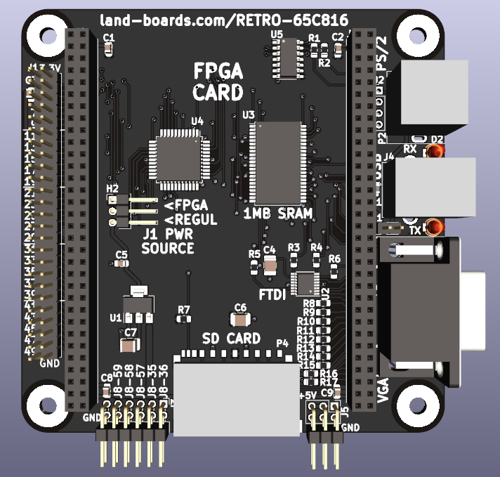
Features
- Design based on RETRO-EP4CE15 card
- Adds 65C816 CPU
- 5V level translator for keyboard
- 5V header moved to board edge
- 65C816 CPU
- 3.3V
- 8 MHz
- All pins are brought to FPGA
- Address A0-A15 and Data lines also go directly to the SRAM
- FPGA can have the ROM internally or download it to the SRAM
- 1MB SRAM
- 45nS access time
- USB B
- FTDI USB to TTL
- Tx/Rx LEDs
- VGA
- 3:3:2 R:G:B
- PS/2 keyboard
- 5V KEYBOARD
- Level translator to 3.3V for FPGA
- SD card socket
- Full-sized SD
- QMTECH FPGA card mounts on top
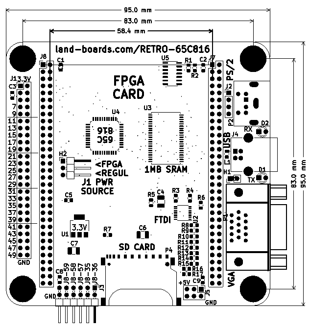
- 95x95mm card
- ODAS form factor
- (4) 6-32 Mounting holes
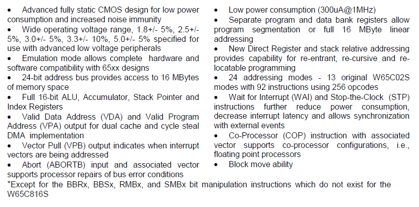
65C816 CPU
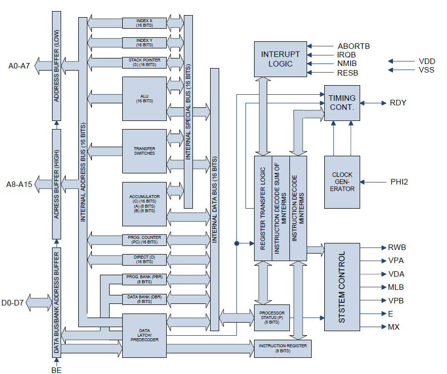
Block Diagram
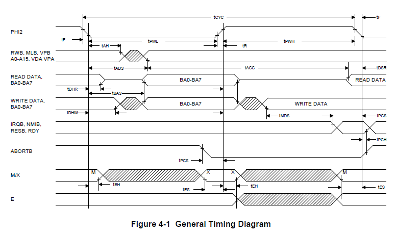
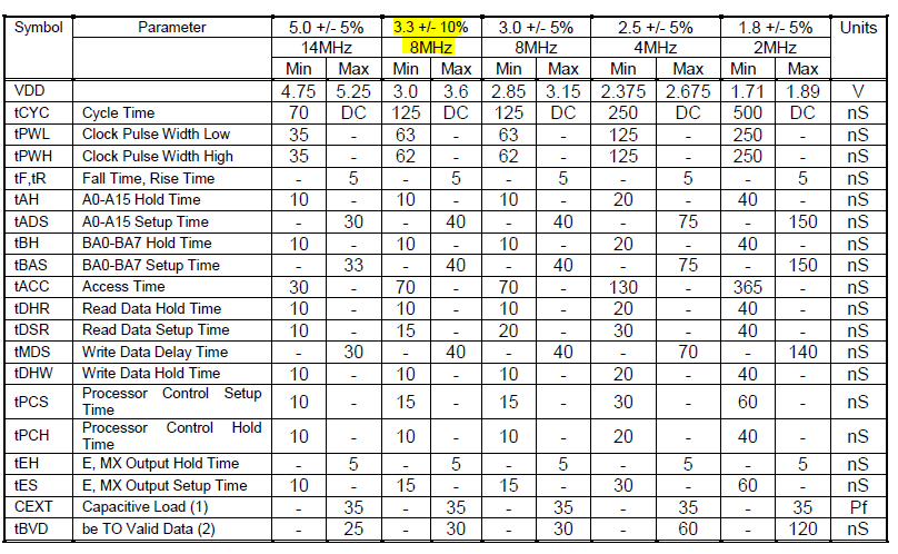
Timing
Connectors
H1 - 5V
- Install jumper to power card from USB
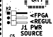
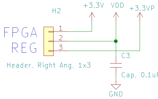
H2 - VREG I/O Conn
- Power to J1
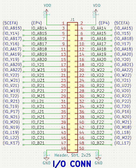
J1 - I/O Connector
- 50-pin I/O Connector
J2 - Keyboard
- 1x4 header
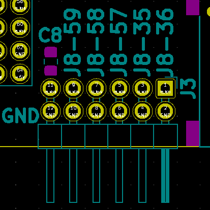
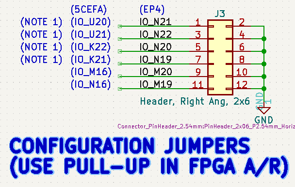
J3 - 6 FPGA pins
J4 - USB B Serial/Power
- Serial to/from FTDI
- Can power the card
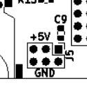
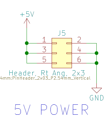
J5 - 5V/GND
- 5V/ground for external 5V logic
J7 Pin Mapping Card to FPGA pins - Right connector
| U7 PIN | EP4CE15 | EP4CE55 | 5CEFA2 | CYC 10 | FUNCTION | U7 PIN | EP4CE15 | EP4CE55 | 5CEFA2 | CYC 10 | FUNCTION | |
|---|---|---|---|---|---|---|---|---|---|---|---|---|
| 1 | GND | GND | GND | GND | GND | 2 | GND | GND | GND | GND | GND | |
| 3 | 3.3V | 3.3V | 3.3V | 3.3V | 3.3V | 4 | 3.3V | 3.3V | 3.3V | 3.3V | 3.3V | |
| 5 | GND | GND | GND | GND | GND | 6 | GND | GND | GND | GND | GND | |
| 7 | PIN_R1 | PIN_R1 | PIN_AA2 | PIN_G1 | PS2CLK | 8 | PIN_R2 | PIN_R2 | PIN_AA1 | PIN_G2 | PS2DAT | |
| 9 | PIN_P1 | PIN_P1 | PIN_Y3 | PIN_D1 | SRAMA4 | 10 | PIN_P2 | PIN_P2 | PIN_W2 | PIN_C2 | SRAMA5 | |
| 11 | PIN_N1 | PIN_N1 | PIN_U1 | PIN_B1 | SRAMA3 | 12 | PIN_N2 | PIN_N2 | PIN_U2 | PIN_F5 | SRAMA6 | |
| 13 | PIN_M1 | PIN_M1 | PIN_N1 | PIN_D3 | SRAMA2 | 14 | PIN_M2 | PIN_M2 | PIN_N2 | PIN_C3 | SRAMA7 | |
| 15 | PIN_J1 | PIN_J1 | PIN_L1 | PIN_B3 | SRAMA1 | 16 | PIN_J2 | PIN_J2 | PIN_L2 | PIN_A3 | SRAM0E_N | |
| 17 | PIN_H1 | PIN_H1 | PIN_G1 | PIN_B4 | SRAMA0 | 18 | PIN_H2 | PIN_H2 | PIN_G2 | PIN_A4 | SRAMA8 | |
| 19 | PIN_F1 | PIN_F1 | PIN_E2 | PIN_E5 | SRAMCS_N | 20 | PIN_F2 | PIN_F2 | PIN_D3 | PIN_A2 | SRAMD7 | |
| 21 | PIN_E1 | PIN_E1 | PIN_C1 | PIN_D4 | SRAMD0 | 22 | PIN_D2 | PIN_D2 | PIN_C2 | PIN_E6 | SRAMD6 | |
| 23 | PIN_C1 | PIN_C1 | PIN_G6 | PIN_C6 | SRAMD1 | 24 | PIN_C2 | PIN_C2 | PIN_H6 | PIN_D6 | SRAMD5 | |
| 25 | PIN_B1 | PIN_B1 | PIN_G8 | PIN_B5 | SRAMD2 | 26 | PIN_B2 | PIN_B2 | PIN_H8 | PIN_A5 | SRAMD4 | |
| 27 | PIN_B3 | PIN_B3 | PIN_F7 | PIN_B6 | SRAMD3 | 28 | PIN_A3 | PIN_A3 | PIN_E7 | PIN_A6 | SRAMA9 | |
| 29 | PIN_B4 | PIN_B4 | PIN_D6 | PIN_B7 | SRAMWE_N | 30 | PIN_A4 | PIN_A4 | PIN_C6 | PIN_A7 | SRAMA10 | |
| 31 | PIN_C4 | PIN_C4 | PIN_E9 | PIN_D8 | SRAMA19 | 32 | PIN_C3 | PIN_C3 | PIN_D9 | PIN_C8 | SRAMA11 | |
| 33 | PIN_B5 | PIN_B5 | PIN_B5 | PIN_D9 | SRAMA18 | 34 | PIN_A5 | PIN_A5 | PIN_A5 | PIN_C9 | SRAMA12 | |
| 35 | PIN_B6 | PIN_B6 | PIN_B6 | PIN_B8 | SRAMA17 | 36 | PIN_A6 | PIN_A6 | PIN_B7 | PIN_A8 | SRAMA13 | |
| 37 | PIN_B7 | PIN_B7 | PIN_A7 | PIN_B9 | SRAMA16 | 38 | PIN_A7 | PIN_A7 | PIN_A8 | PIN_A9 | SRAMA14 | |
| 39 | PIN_B8 | PIN_B8 | PIN_A9 | PIN_E9 | N/C | 40 | PIN_A8 | PIN_A8 | PIN_A10 | PIN_E8 | SRAMA15 | |
| 41 | PIN_B9 | PIN_B9 | PIN_B10 | PIN_E11 | CARDDET | 42 | PIN_A9 | PIN_A9 | PIN_C9 | PIN_E10 | N/C | |
| 43 | PIN_B10 | PIN_B10 | PIN_G10 | PIN_A10 | USBRX/o_FPGATX | 44 | PIN_A10 | PIN_A10 | PIN_F10 | PIN_B10 | USBCTS/o_FPGARTS | |
| 45 | PIN_B13 | PIN_B13 | PIN_C11 | PIN_D12 | USBTX/i_FPGARX | 46 | PIN_A13 | PIN_A13 | PIN_B11 | PIN_D11 | UBSRTS/i_FPGACTS | |
| 47 | PIN_B14 | PIN_B14 | PIN_B12 | PIN_B11 | REDHI | 48 | PIN_A14 | PIN_A14 | PIN_A12 | PIN_A11 | REDMID | |
| 49 | PIN_B15 | PIN_B15 | PIN_E12 | PIN_B12 | REDLO | 50 | PIN_A15 | PIN_A15 | PIN_D12 | PIN_A12 | GRNHI | |
| 51 | PIN_B16 | PIN_B16 | PIN_D13 | PIN_B13 | GRNMID | 52 | PIN_A16 | PIN_A16 | PIN_C13 | PIN_A13 | GRNLO | |
| 53 | PIN_B17 | PIN_B17 | PIN_B13 | PIN_B14 | BLUHI | 54 | PIN_A17 | PIN_A17 | PIN_A13 | PIN_A14 | BLULO | |
| 55 | PIN_B18 | PIN_B18 | PIN_A15 | PIN_D14 | HSYNC | 56 | PIN_A18 | PIN_A18 | PIN_A14 | PIN_C14 | VSYNC | |
| 57 | PIN_B19 | PIN_B19 | PIN_B15 | PIN_B16 | SDCS_N | 58 | PIN_A19 | PIN_A19 | PIN_C15 | PIN_A15 | SD_MOSI | |
| 59 | PIN_B20 | PIN_B20 | PIN_C16 | PIN_C16 | SD_SCK | 60 | PIN_A20 | PIN_A20 | PIN_B16 | PIN_C15 | SD_MISO | |
| 61 | GND | GND | GND | GND | GND | 62 | GND | GND | GND | GND | GND | |
| 63 | VIN | VIN | VIN | VIN | VIN | 64 | VIN | VIN | VIN | VIN | VIN |
J8 Pin Mapping Card to FPGA pins - Left connector
- Cyclone 10 notes
- Cannot place output or bidirectional pin J8IO[35] in input pin location M16
- Cannot place output or bidirectional pin J8IO[36] in input pin location M15
- Cannot place output or bidirectional pin J8IO[57] in input pin location E16
- Cannot place output or bidirectional pin J8IO[58] in input pin location E15
| U8 PIN | EP4CE15 | EP4CE55 | 5CEFA2 | 10C1006 | J1 | Function | U8 PIN | EP4CE15 | EP4CE55 | 5CEFA2 | 10C1006 | J1 | Function | |
|---|---|---|---|---|---|---|---|---|---|---|---|---|---|---|
| 1 | GND | GND | GND | GND | N/C | 2 | GND | GND | GND | GND | N/C | |||
| 3 | 3.3V | 3.3V | 3.3V | 3.3V | J1-1 | 4 | 3.3V | 3.3V | 3.3V | 3.3V | J1-2 | |||
| 5 | GND | GND | GND | GND | N/C | 6 | GND | GND | GND | GND | N/C | |||
| 7 | PIN_AA13 | PIN_AA13 | PIN_AA14 | PIN_R9 | N/C | CPUE | 8 | PIN_AB13 | PIN_AB13 | PIN_AA13 | PIN_T9 | N/C | CPURES* | |
| 9 | PIN_AA14 | PIN_AA14 | PIN_AA15 | PIN_R10 | J1-4 | CPUMX | 10 | PIN_AB14 | PIN_AB14 | PIN_AB15 | PIN_T10 | J1-3 | CPUCLK | |
| 11 | PIN_AA15 | PIN_AA15 | PIN_Y15 | PIN_R11 | J1-6 | CPUBE | 12 | PIN_AB15 | PIN_AB15 | PIN_Y13 | PIN_T11 | J1-5 | CPUNMIB | |
| 13 | PIN_AA16 | PIN_AA16 | PIN_AB18 | PIN_R12 | J1-8 | CPURWB | 14 | PIN_AB16 | PIN_AB16 | PIN_AB17 | PIN_T12 | J1-7 | CPUIRQB | |
| 15 | PIN_AA17 | PIN_AA17 | PIN_Y7 | PIN_N9 | J1-10 | CPUVDA | 16 | PIN_AB17 | PIN_AB17 | PIN_Y16 | PIN_M9 | J1-9 | CPUABORTB | |
| 17 | PIN_AA18 | PIN_AA18 | PIN_AA18 | PIN_M10 | J1-12 | CPUVPA | 18 | PIN_AB18 | PIN_AB18 | PIN_AA17 | PIN_P9 | J1-11 | CPURDY | |
| 19 | PIN_AA19 | PIN_AA19 | PIN_AA20 | PIN_P11 | J1-14 | CPUVPB | 20 | PIN_AB19 | PIN_AB19 | PIN_AA19 | PIN_N11 | J1-13 | CPUMLB | |
| 21 | PIN_AA20 | PIN_AA20 | PIN_Y20 | PIN_R13 | I1-16 | 22 | PIN_AB20 | PIN_AB20 | PIN_Y19 | PIN_T13 | J1-15 | |||
| 23 | PIN_Y22 | PIN_Y22 | PIN_AB21 | PIN_T15 | J1-18 | 24 | PIN_Y21 | PIN_Y21 | PIN_AB20 | PIN_T14 | J1-17 | |||
| 25 | PIN_W22 | PIN_W22 | PIN_AA22 | PIN_N12 | J1-20 | 26 | PIN_W21 | PIN_W21 | PIN_AB22 | PIN_M11 | J1-19 | |||
| 27 | PIN_V22 | PIN_V22 | PIN_W22 | PIN_R14 | J1-22 | 28 | PIN_V21 | PIN_V21 | PIN_Y22 | PIN_N13 | J1-21 | |||
| 29 | PIN_U22 | PIN_U22 | PIN_Y21 | PIN_N14 | J1-24 | 30 | PIN_U21 | PIN_U21 | PIN_W21 | PIN_P14 | J1-23 | |||
| 31 | PIN_R22 | PIN_R22 | PIN_U22 | PIN_P16 | J1-26 | 32 | PIN_R21 | PIN_R21 | PIN_V21 | PIN_R16 | J1-25 | |||
| 33 | PIN_P22 | PIN_P22 | PIN_V20 | PIN_N16 | J1-28 | 34 | PIN_P21 | PIN_P21 | PIN_W19 | PIN_N15 | J1-27 | |||
| 35 | PIN_N22 | PIN_N22 | PIN_U21 | PIN_M16 (Note) | J3-3 | 36 | PIN_N21 | PIN_N21 | PIN_U20 | PIN_M15 (Note) | J3-1 | |||
| 37 | PIN_M22 | PIN_M22 | PIN_R22 | PIN_L16 | J1-30 | 38 | PIN_M21 | PIN_M21 | PIN_T22 | PIN_L15 | J1-29 | |||
| 39 | PIN_L22 | PIN_L22 | PIN_P22 | PIN_P15 | J1-32 | 40 | PIN_L21 | PIN_L21 | PIN_R21 | PIN_M12 | J1-31 | |||
| 41 | PIN_K22 | PIN_K22 | PIN_T20 | PIN_L14 | J1-34 | 42 | PIN_K21 | PIN_K21 | PIN_T19 | PIN_L13 | J1-33 | |||
| 43 | PIN_J22 | PIN_J22 | PIN_P16 | PIN_K16 | J1-36 | 44 | PIN_J21 | PIN_J21 | PIN_P17 | PIN_K15 | J1-35 | |||
| 45 | PIN_H22 | PIN_H22 | PIN_N20 | PIN_K12 | J1-38 | 46 | PIN_H21 | PIN_H21 | PIN_N21 | PIN_J12 | J1-37 | |||
| 47 | PIN_F22 | PIN_F22 | PIN_M21 | PIN_J14 | J1-40 | 48 | PIN_F21 | PIN_F21 | PIN_M20 | PIN_J13 | J1-39 | |||
| 49 | PIN_E22 | PIN_E22 | PIN_M18 | PIN_K11 | J1-42 | 50 | PIN_E21 | PIN_E21 | PIN_N19 | PIN_J11 | J1-41 | |||
| 51 | PIN_D22 | PIN_D22 | PIN_L18 | PIN_G11 | J1-44 | 52 | PIN_D21 | PIN_D21 | PIN_L19 | PIN_F11 | J1-43 | |||
| 53 | PIN_C22 | PIN_C22 | PIN_M22 | PIN_F13 | J1-46 | 54 | PIN_C21 | PIN_C21 | PIN_L22 | PIN_F14 | J1-45 | |||
| 55 | PIN_B22 | PIN_B22 | PIN_L17 | PIN_F10 | J1-48 | 56 | PIN_B21 | PIN_B21 | PIN_K17 | PIN_F9 | J1-47 | |||
| 57 | PIN_N20 | PIN_N20 | PIN_K22 | PIN_E16 (Note) | J3-5 | 58 | PIN_N19 | PIN_N19 | PIN_K21 | PIN_E15 (Note) | J3-7 | |||
| 59 | PIN_M20 | PIN_M20 | PIN_M16 | PIN_D16 | J3-9 | 60 | PIN_M19 | PIN_M19 | PIN_N16 | PIN_D15 | J3-11 | |||
| 61 | GND | GND | GND | GND | J1-50 | 62 | GND | GND | GND | GND | J1-49 | |||
| 63 | +5V | +5V | +5V | +5V | J1-50 | 64 | +5V | +5V | +5V | +5V | J1-50 |
P1 - VGA
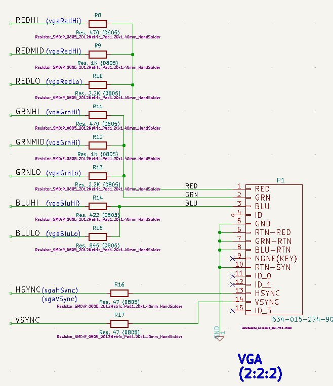
- DB-15HD connector
- 3:3:2 R:G:B
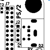
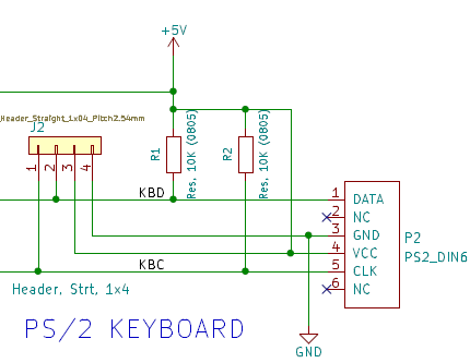
P2 - PS/2 Keyboard
- Purple DIN-6 for PS/2 keyboard
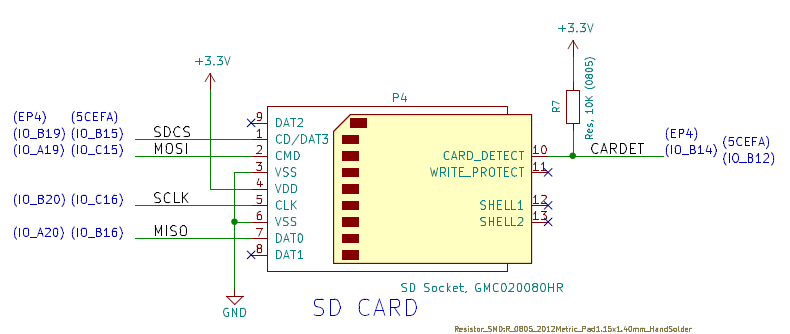
P4 - SD Card
Mechanicals
MultiComp On RETRO-65C816 VHDL Code
References/Notes
- On the usefulness of 65816 as a 65C02 alternative
- Helpful timing information
...potential for data bus contention during Ø2 low. My solution was two-fold: use VDA and VPA to qualify chip selects, and qualify read-accesses with Ø2. The former assures that an addressed device will not respond to selection until the address bus is truly valid—invalid bus states may occur during the execution of some instructions. The latter assures that a selected device will not drive the data bus when the '816 is presenting A16-A23 on it. This solution doesn't totally eliminate the risk of contention but greatly narrows the window of opportunity for it. The need for more stringent qualifying of D0-D7 would depend on the peripheral silicon on the bus. In the case of POC and the Ø2 rate I'm using (12.5 MHz maximum), everything gets off the data bus before the '816 starts to drive it with the bank address. That would not be the case if I were to increase Ø2 to 20 MHz, however.

Floating the buses with BE creates the odd situation where no valid address exists on A0-A15, which I daresay could cause a device to be selected solely because of a residual charge in bus capacitance. Also, BE floats the RWB signal*, which may trip up other logic that is dependent on RWB always being driven to one state or the other. The most fool-proof solution is the use of a data bus transceiver as you suggested, which is a straightforward method (74AC245 or 74AHC245 recommended if Ø2 will exceed 8 MHz).
Pin List (10CL006YU256C8G)
set_global_assignment -name FAMILY "Cyclone 10 LP"
set_global_assignment -name DEVICE 10CL006YU256C8G
set_global_assignment -name TOP_LEVEL_ENTITY M6502_VGA
set_global_assignment -name ORIGINAL_QUARTUS_VERSION "13.0 SP1"
set_global_assignment -name PROJECT_CREATION_TIME_DATE "18:01:55  MARCH 31, 2019"
set_global_assignment -name LAST_QUARTUS_VERSION "21.1.0 Lite Edition"
set_global_assignment -name PROJECT_OUTPUT_DIRECTORY output_files
set_global_assignment -name MIN_CORE_JUNCTION_TEMP 0
set_global_assignment -name MAX_CORE_JUNCTION_TEMP 85
set_global_assignment -name ERROR_CHECK_FREQUENCY_DIVISOR 1
set_global_assignment -name PARTITION_NETLIST_TYPE SOURCE -section_id Top
set_global_assignment -name PARTITION_FITTER_PRESERVATION_LEVEL PLACEMENT_AND_ROUTING -section_id Top
set_global_assignment -name PARTITION_COLOR 16764057 -section_id Top
set_global_assignment -name POWER_PRESET_COOLING_SOLUTION "23 MM HEAT SINK WITH 200 LFPM AIRFLOW"
set_global_assignment -name POWER_BOARD_THERMAL_MODEL "NONE (CONSERVATIVE)"
set_global_assignment -name STRATIX_DEVICE_IO_STANDARD "3.3-V LVTTL"
set_global_assignment -name USE_CONFIGURATION_DEVICE OFF
set_global_assignment -name CRC_ERROR_OPEN_DRAIN OFF
set_global_assignment -name OUTPUT_IO_TIMING_NEAR_END_VMEAS "HALF VCCIO" -rise
set_global_assignment -name OUTPUT_IO_TIMING_NEAR_END_VMEAS "HALF VCCIO" -fall
set_global_assignment -name OUTPUT_IO_TIMING_FAR_END_VMEAS "HALF SIGNAL SWING" -rise
set_global_assignment -name OUTPUT_IO_TIMING_FAR_END_VMEAS "HALF SIGNAL SWING" -fall
set_global_assignment -name CYCLONEII_RESERVE_NCEO_AFTER_CONFIGURATION "USE AS REGULAR IO"
# Clock, reset switch
set_location_assignment PIN_E1 -to i_clk_50
set_location_assignment PIN_J6 -to i_n_reset
set_instance_assignment -name WEAK_PULL_UP_RESISTOR ON -to i_n_reset
# PS/2 keyboard
set_location_assignment PIN_G1 -to io_ps2Clk
set_instance_assignment -name WEAK_PULL_UP_RESISTOR ON -to io_ps2Clk
set_location_assignment PIN_G2 -to io_ps2Data
set_instance_assignment -name WEAK_PULL_UP_RESISTOR ON -to io_ps2Data
# Serial port with RTS/CTS
set_location_assignment PIN_D11 -to i_n_cts
set_location_assignment PIN_D12 -to i_rxd
set_instance_assignment -name WEAK_PULL_UP_RESISTOR ON -to i_rxd
set_location_assignment PIN_B10 -to o_n_rts
set_location_assignment PIN_A10 -to o_txd
# Video
set_location_assignment PIN_B12 -to o_vid_red[0]
set_location_assignment PIN_A11 -to o_vid_red[1]
set_location_assignment PIN_B11 -to o_vid_red[2]
set_location_assignment PIN_A13 -to o_vid_grn[0]
set_location_assignment PIN_B13 -to o_vid_grn[1]
set_location_assignment PIN_A12 -to o_vid_grn[2]
set_location_assignment PIN_A14 -to o_vid_blu[0]
set_location_assignment PIN_B14 -to o_vid_blu[1]
set_location_assignment PIN_D14 -to o_vid_hSync
set_location_assignment PIN_C14 -to o_vid_vSync
# SRAM
set_location_assignment PIN_E5 -to o_n_sRamCS
set_location_assignment PIN_A3 -to o_n_sRamOE
set_location_assignment PIN_B7 -to o_n_sRamWE
set_location_assignment PIN_D4 -to io_sramData[0]
set_location_assignment PIN_C6 -to io_sramData[1]
set_location_assignment PIN_B5 -to io_sramData[2]
set_location_assignment PIN_B6 -to io_sramData[3]
set_location_assignment PIN_A5 -to io_sramData[4]
set_location_assignment PIN_D6 -to io_sramData[5]
set_location_assignment PIN_E6 -to io_sramData[6]
set_location_assignment PIN_A2 -to io_sramData[7]
set_location_assignment PIN_B4 -to o_sramAddress[0]
set_location_assignment PIN_B3 -to o_sramAddress[1]
set_location_assignment PIN_D3 -to o_sramAddress[2]
set_location_assignment PIN_B1 -to o_sramAddress[3]
set_location_assignment PIN_D1 -to o_sramAddress[4]
set_location_assignment PIN_C2 -to o_sramAddress[5]
set_location_assignment PIN_F5 -to o_sramAddress[6]
set_location_assignment PIN_C3 -to o_sramAddress[7]
set_location_assignment PIN_A4 -to o_sramAddress[8]
set_location_assignment PIN_A6 -to o_sramAddress[9]
set_location_assignment PIN_A7 -to o_sramAddress[10]
set_location_assignment PIN_C8 -to o_sramAddress[11]
set_location_assignment PIN_C9 -to o_sramAddress[12]
set_location_assignment PIN_A8 -to o_sramAddress[13]
set_location_assignment PIN_A9 -to o_sramAddress[14]
set_location_assignment PIN_E8 -to o_sramAddress[15]
set_location_assignment PIN_B9 -to o_sramAddress[16]
set_location_assignment PIN_B8 -to o_sramAddress[17]
set_location_assignment PIN_D9 -to o_sramAddress[18]
set_location_assignment PIN_D8 -to o_sramAddress[19]
# SD Card
set_location_assignment PIN_B16 -to sdCS
set_location_assignment PIN_C15 -to sdMISO
set_instance_assignment -name WEAK_PULL_UP_RESISTOR ON -to sdMISO
set_location_assignment PIN_A15 -to sdMOSI
set_location_assignment PIN_C16 -to sdClock
set_location_assignment PIN_E11 -to i_n_CardDet
set_instance_assignment -name WEAK_PULL_UP_RESISTOR ON -to i_n_CardDet
set_location_assignment PIN_L9 -to driveLED
# SDRAM
set_location_assignment PIN_P2 -to sdRamClk
set_location_assignment PIN_R1 -to sdRamClkEn
set_location_assignment PIN_M7 -to n_sdRamCas
set_location_assignment PIN_P8 -to n_sdRamCe
set_location_assignment PIN_M8 -to n_sdRamRas
set_location_assignment PIN_P6 -to n_sdRamWe
set_location_assignment PIN_R7 -to sdRamAddr[0]
set_location_assignment PIN_T7 -to sdRamAddr[1]
set_location_assignment PIN_R8 -to sdRamAddr[2]
set_location_assignment PIN_T8 -to sdRamAddr[3]
set_location_assignment PIN_R6 -to sdRamAddr[4]
set_location_assignment PIN_T5 -to sdRamAddr[5]
set_location_assignment PIN_R5 -to sdRamAddr[6]
set_location_assignment PIN_T4 -to sdRamAddr[7]
set_location_assignment PIN_R4 -to sdRamAddr[8]
set_location_assignment PIN_T3 -to sdRamAddr[9]
set_location_assignment PIN_T6 -to sdRamAddr[10]
set_location_assignment PIN_R3 -to sdRamAddr[11]
set_location_assignment PIN_T2 -to sdRamAddr[12]
set_location_assignment PIN_N8 -to sdRamAddr[13]
set_location_assignment PIN_L8 -to sdRamAddr[14]
set_location_assignment PIN_K5 -to sdRamData[0]
set_location_assignment PIN_L3 -to sdRamData[1]
set_location_assignment PIN_L4 -to sdRamData[2]
set_location_assignment PIN_K6 -to sdRamData[3]
set_location_assignment PIN_N3 -to sdRamData[4]
set_location_assignment PIN_M6 -to sdRamData[5]
set_location_assignment PIN_P3 -to sdRamData[6]
set_location_assignment PIN_N5 -to sdRamData[7]
set_location_assignment PIN_N2 -to sdRamData[8]
set_location_assignment PIN_N1 -to sdRamData[9]
set_location_assignment PIN_L1 -to sdRamData[10]
set_location_assignment PIN_L2 -to sdRamData[11]
set_location_assignment PIN_K1 -to sdRamData[12]
set_location_assignment PIN_K2 -to sdRamData[13]
set_location_assignment PIN_J1 -to sdRamData[14]
set_location_assignment PIN_J2 -to sdRamData[15]
#
set_location_assignment PIN_R13 -to IO_PIN[16]
set_location_assignment PIN_T13 -to IO_PIN[17]
set_location_assignment PIN_T15 -to IO_PIN[18]
set_location_assignment PIN_T14 -to IO_PIN[19]
set_location_assignment PIN_N12 -to IO_PIN[20]
set_location_assignment PIN_L15 -to IO_PIN[29]
set_location_assignment PIN_L16 -to IO_PIN[30]
set_location_assignment PIN_N13 -to IO_PIN[21]
set_location_assignment PIN_R14 -to IO_PIN[22]
set_location_assignment PIN_P14 -to IO_PIN[23]
set_location_assignment PIN_N14 -to IO_PIN[24]
set_location_assignment PIN_R16 -to IO_PIN[25]
set_location_assignment PIN_P16 -to IO_PIN[26]
set_location_assignment PIN_N15 -to IO_PIN[27]
set_location_assignment PIN_N16 -to IO_PIN[28]
set_location_assignment PIN_M12 -to IO_PIN[31]
set_location_assignment PIN_P15 -to IO_PIN[32]
set_location_assignment PIN_L13 -to IO_PIN[33]
set_location_assignment PIN_L14 -to IO_PIN[34]
set_location_assignment PIN_K15 -to IO_PIN[35]
set_location_assignment PIN_K16 -to IO_PIN[36]
set_location_assignment PIN_J12 -to IO_PIN[37]
set_location_assignment PIN_K12 -to IO_PIN[38]
set_location_assignment PIN_J13 -to IO_PIN[39]
set_location_assignment PIN_J14 -to IO_PIN[40]
set_location_assignment PIN_J11 -to IO_PIN[41]
set_location_assignment PIN_K11 -to IO_PIN[42]
set_location_assignment PIN_F11 -to IO_PIN[43]
set_location_assignment PIN_G11 -to IO_PIN[44]
set_location_assignment PIN_F14 -to IO_PIN[45]
set_location_assignment PIN_F13 -to IO_PIN[46]
set_location_assignment PIN_F9 -to IO_PIN[47]
set_location_assignment PIN_F10 -to IO_PIN[48]
#
set_location_assignment PIN_M15 -to J3_IO[0]
set_location_assignment PIN_M16 -to J3_IO[1]
set_location_assignment PIN_E16 -to J3_IO[2]
set_location_assignment PIN_E15 -to J3_IO[3]
set_location_assignment PIN_D16 -to J3_IO[4]
set_location_assignment PIN_D15 -to J3_IO[5]
#
set_location_assignment PIN_R9 -to CPU_E
set_location_assignment PIN_T9 -to n_CPU_Res
set_location_assignment PIN_R10 -to CPU_MX
set_location_assignment PIN_T10 -to CPU_CLK
set_location_assignment PIN_R11 -to CPU_BusEnable
set_location_assignment PIN_T11 -to CPU_NMIB
set_location_assignment PIN_R12 -to CPU_RWB
set_location_assignment PIN_T12 -to CPU_IRQB
set_location_assignment PIN_N9 -to CPU_VDA
set_location_assignment PIN_M9 -to CPU_ABORTB
set_location_assignment PIN_M10 -to CPU_VPA
set_location_assignment PIN_P9 -to CPU_RDY
set_location_assignment PIN_P11 -to CPU_VPB
set_location_assignment PIN_N11 -to CPU_MLB
Revision History
Rev 2
- Fixed W65C816 footprint
- Bigger footprint
- Moved around a lot of tracks to remove ground trace and use ground plane
- Changed from 2:2:2 to 3:3:2 bit video (256 colors)
- Changed J1 pinout to not use (2) input-only J8 pins
- Shuffled J7 pinout to add video bits
- Shuffled J8 to skip Cyclone 10 input-only pins
- Moved to J3 (now has 4 input-only pins and 2 I/O pins)
Rev 1
- RETRO-65C816 Rev 1
- W65C816 footprint is too small for part
- Used TQFP footprint but part is clearly too big
- Datasheet does not indicate package detail
- 0.8mm pitch was OK
- Works well as RETRO-EP4CE15 replacement
- PS/2 @5V is good
Videos
- 65C816 Computer 27 Videos Series - Adrien Kohlbecker
- Lot of detail on 65C816 hardware
