Difference between revisions of "ODAS-PSOC5"
Jump to navigation
Jump to search
Blwikiadmin (talk | contribs) |
Blwikiadmin (talk | contribs) |
||
| (35 intermediate revisions by the same user not shown) | |||
| Line 1: | Line 1: | ||
[[File:tindie-mediums.png|link=https://www.tindie.com/products/land_boards/programmable-system-on-a-chip-odas-psoc5/]] | [[File:tindie-mediums.png|link=https://www.tindie.com/products/land_boards/programmable-system-on-a-chip-odas-psoc5/]] | ||
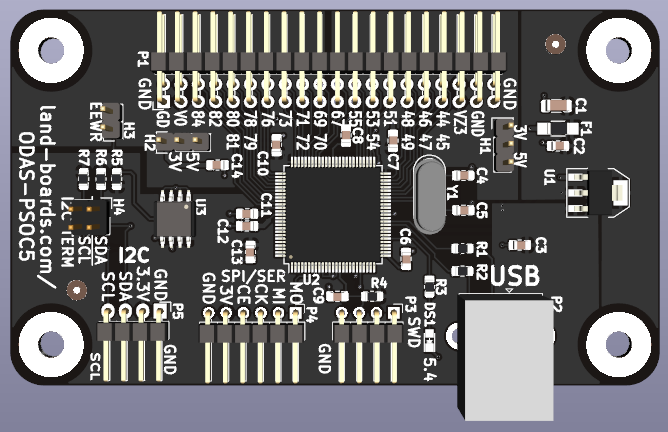
| − | + | [[file:ODAS-PSOC5_FRONT_3D.png]] | |
| − | [[file:ODAS- | ||
<video type="youtube">DijfV5AAAg4</video> | <video type="youtube">DijfV5AAAg4</video> | ||
| Line 8: | Line 7: | ||
== Features == | == Features == | ||
| + | * See here for [[ODAS-PSOC5 Rev X1-X4]] | ||
* PSOC5 Programmable System on a Chip | * PSOC5 Programmable System on a Chip | ||
** Part number: [https://www.infineon.com/cms/en/product/microcontroller/32-bit-psoc-arm-cortex-microcontroller/32-bit-psoc-5-lp-arm-cortex-m3/cy8c52lpxxx/cy8c5267axi-lp051/ CY8C5267AXI-LP051] | ** Part number: [https://www.infineon.com/cms/en/product/microcontroller/32-bit-psoc-arm-cortex-microcontroller/32-bit-psoc-5-lp-arm-cortex-m3/cy8c52lpxxx/cy8c5267axi-lp051/ CY8C5267AXI-LP051] | ||
| Line 13: | Line 13: | ||
** Data Bus Width: 32 bit | ** Data Bus Width: 32 bit | ||
** Maximum Clock Frequency: 67 MHz | ** Maximum Clock Frequency: 67 MHz | ||
| − | ** Program Memory | + | ** Program Memory Type: Flash, 128 kB |
| − | ** Data RAM | + | ** Data RAM: SRAM, 32 kB |
| − | ** ADC Resolution: 12 bit | + | ** ADC |
| − | ** | + | *** Resolution: 12 bit SAR |
| − | ** | + | *** Number of ADC Channels: 1 |
| − | ** Number of | + | ** 8-bit DAC |
| + | ** Number of Timers/Counters: 4 Timers | ||
** Number of I/Os: 72 I/O | ** Number of I/Os: 72 I/O | ||
| − | ** | + | *** Interface Types: I2C, USB, SPI |
| − | ** | + | ** Programmable Analog and Digital sections |
* 16 MHz External Crystal | * 16 MHz External Crystal | ||
* Connectors | * Connectors | ||
| Line 29: | Line 30: | ||
** I2C Connector (4-pin header) | ** I2C Connector (4-pin header) | ||
** SPI Connector (6-pin header) | ** SPI Connector (6-pin header) | ||
| − | * [https://www.mouser.com/ProductDetail/579-24LC024-P 24LC024 | + | * [[Open_Data_Acquisition_System#Personality_EEPROM|ODAS Personality EEPROM]] |
| + | ** [https://www.mouser.com/ProductDetail/579-24LC024-P 24LC024] | ||
** pid = 8 | ** pid = 8 | ||
** Write protect jumper | ** Write protect jumper | ||
* On Board LED (5.4) | * On Board LED (5.4) | ||
| − | * | + | * Power input on USB B connector |
| − | ** On-board 3.3V | + | ** On-board 3.3V regulator |
| − | ** | + | ** Polysilicon fuse on 3.3V power |
| − | * | + | * 95x55mm ODAS Form Factor |
* Compatible with Land Boards [[Open Data Acquisition System]] (ODAS) Cards | * Compatible with Land Boards [[Open Data Acquisition System]] (ODAS) Cards | ||
* (4) #6 screw holes for solid mounting | * (4) #6 screw holes for solid mounting | ||
| + | |||
| + | === CY8C5267AXI-LP051 Features === | ||
| + | |||
| + | [[file:PSoC5LP_Devices_CY8C5267AXI-LP051.png]] | ||
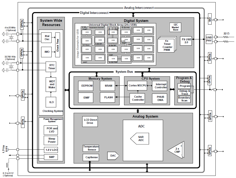
=== PSoC Architecture === | === PSoC Architecture === | ||
| − | [[file: | + | [[file:PSOC5_BlockDiagram.PNG]] |
== Headers == | == Headers == | ||
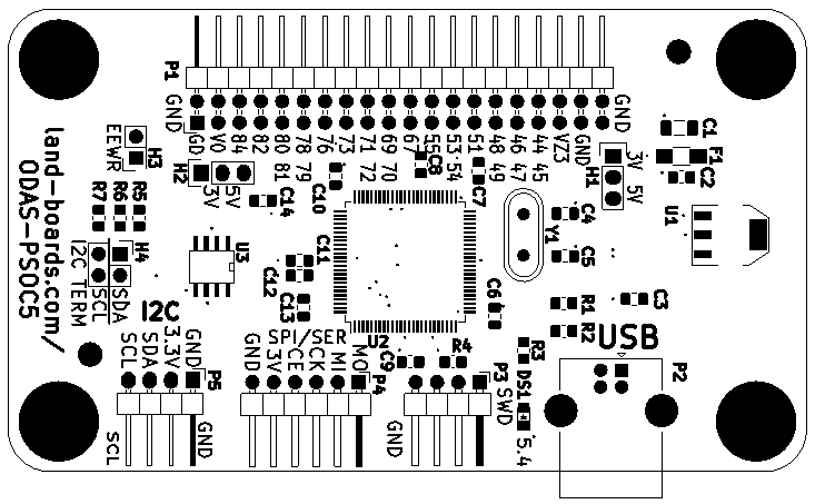
| − | + | [[file:ODAS-PSOC5-CAD-REV-5.PNG]] | |
| − | |||
| − | [[ | ||
| − | |||
| − | |||
| − | |||
| − | |||
| − | |||
| − | |||
| − | |||
| − | |||
| − | |||
| − | |||
| − | |||
| − | === | + | === H1 - I/O Voltage Zone 3 (VZ3) === |
| − | [[FILE: | + | [[FILE:ODAS-PSOC5_Rev5_H1.PNG]] |
* 1-2 = 3.3V | * 1-2 = 3.3V | ||
| Line 69: | Line 62: | ||
* Connects to J1 VZ3 pins | * Connects to J1 VZ3 pins | ||
| − | === | + | === H2 - I/O Voltage Zone 0 (VZ0) === |
| − | [[FILE: | + | [[FILE:ODAS-PSOC5_Rev5_H2.PNG]] |
* 1-2 = 3.3V | * 1-2 = 3.3V | ||
| Line 77: | Line 70: | ||
* Connects to J1 VZ0 pins | * Connects to J1 VZ0 pins | ||
| − | == | + | === H3 - EEPROM Write Enable === |
| − | + | [[FILE:ODAS-PSOC5_Rev5_H3.PNG]] | |
| − | * | + | * Install to enable EEPROM writes |
| − | |||
| − | |||
| − | === | + | === H4 - I2C Terminator === |
| − | * | + | [[FILE:ODAS-PSOC5_Rev5_H4.PNG]] |
| − | * | + | |
| + | * Install headers to enable terminators | ||
| + | * 1-2 SDA 3.3K Terminator | ||
| + | * 3-4 SCL 3.3K Terminator | ||
| + | |||
| + | == Connectors == | ||
| + | |||
| + | [[file:ODAS-PSOC5-CAD-REV-5.PNG]] | ||
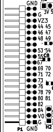
=== P1 - I/O Connector === | === P1 - I/O Connector === | ||
| + | |||
| + | [[file:ODAS-PSOC5_Rev5_P1.PNG]] | ||
{| class="wikitable" | {| class="wikitable" | ||
| Line 214: | Line 214: | ||
|- | |- | ||
| 39 | | 39 | ||
| − | | | + | | GND |
| | | | ||
| 40 | | 40 | ||
| − | | | + | | GND |
|- | |- | ||
|} | |} | ||
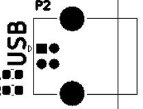
| − | === P2 - | + | === P2 - USB B === |
| − | [[ | + | [[file:ODAS-PSOC5_Rev5_P2.PNG]] |
| − | + | * Power is connected through this connector | |
| − | + | * USB-Serial connection | |
| − | |||
| − | |||
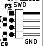
| − | === P3 - | + | === P3 - PSOC SWD Programming Header=== |
| − | [[FILE: | + | [[FILE:ODAS-PSOC5_Rev5_P3.PNG]] |
| − | + | # SWDIO | |
| − | + | # SWDCLK | |
| − | + | # RESET | |
| + | # GND | ||
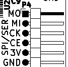
=== P4 - SPI === | === P4 - SPI === | ||
| − | [[FILE: | + | [[FILE:ODAS-PSOC5_Rev5_P4.PNG]] |
# SPI_MOSI | # SPI_MOSI | ||
| Line 248: | Line 247: | ||
# +3.3V | # +3.3V | ||
# GND | # GND | ||
| + | |||
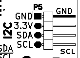
| + | === P5 - I2C Master (or Slave) === | ||
| + | |||
| + | [[FILE:ODAS-PSOC5_Rev5_P5.PNG]] | ||
| + | |||
| + | # GND | ||
| + | # 3.3V | ||
| + | # SDA | ||
| + | # SCL | ||
== Programming == | == Programming == | ||
| Line 294: | Line 302: | ||
** D15, D31 are not used | ** D15, D31 are not used | ||
| − | == | + | == Mechanicals == |
| − | [[file:ODAS-PSOC5- | + | [[file:ODAS-PSOC5-MECHS-REV-5.PNG]] |
== Software == | == Software == | ||
* [https://github.com/land-boards/ODAS/tree/master/ODAS-PSOC5/Projects GitHub Repository] | * [https://github.com/land-boards/ODAS/tree/master/ODAS-PSOC5/Projects GitHub Repository] | ||
| + | |||
| + | == References == | ||
| + | |||
| + | * [https://www.infineon.com/dgdl/Infineon-AN77759_Getting_Started_with_PSoC_5LP-ApplicationNotes-v08_00-EN.pdf?fileId=8ac78c8c7cdc391c017d071b8fb71dc6&utm_source=cypress&utm_medium=referral&utm_campaign=202110_globe_en_all_integration-application_note AN77759 Getting Started with PSoC 5LP] | ||
| + | * [https://www.infineon.com/dgdl/Infineon-AN61290_PSoC_3_and_PSoC_5LP_Hardware_Design_Considerations-ApplicationNotes-v17_00-EN.pdf?fileId=8ac78c8c7cdc391c017d07254f524a25&utm_source=cypress&utm_medium=referral&utm_campaign=202110_globe_en_all_integration-application_note AN61290 PSoC 5LP Hardware Design Considerations] | ||
| + | * [https://www.infineon.com/dgdl/Infineon-AN58304_PSoC_3_and_PSoC_5LP_Pin_Selection_for_Analog_Designs-ApplicationNotes-v09_00-EN.pdf?fileId=8ac78c8c7cdc391c017d072e43f252d4&utm_source=cypress&utm_medium=referral&utm_campaign=202110_globe_en_all_integration-application_note AN58304 PSoC 5LP – Pin Selection for Analog Designs] | ||
| + | * [https://www.infineon.com/dgdl/Infineon-AN81623_PSoC_3_PSoC_4_and_PSoC_5LP_Digital_Design_Best_Practices-ApplicationNotes-v07_00-EN.pdf?fileId=8ac78c8c7cdc391c017d0726b5b94b78&utm_source=cypress&utm_medium=referral&utm_campaign=202110_globe_en_all_integration-application_note AN81623 PSoC 5LP Digital Design Best Practices] | ||
| + | * [https://www.infineon.com/dgdl/Infineon-AN69133_PSoC_3_PSoC_5LP_Easy_Waveform_Generation_with_the_WaveDAC8_Component-ApplicationNotes-v07_00-EN.pdf?fileId=8ac78c8c7cdc391c017d0730b6d05487 AN69133 PSoC 5LP Easy Waveform Generation with the WaveDAC8 Component] | ||
| + | * [https://www.infineon.com/dgdl/Infineon-CE58035-Code%20Example-v01_00-EN.zip?fileId=8ac78c8c7cdc391c017d0d71d4284c27 I2C EEPROM example] | ||
| + | |||
| + | == Revisions == | ||
| + | |||
| + | === Rev 5 === | ||
| + | |||
| + | * Change to USB B connector | ||
| + | ** Power card from 5V through USB B connector | ||
| + | * Remove 5V regulator | ||
| + | * Re-sequence reference designators top to bottom | ||
== Assembly Sheet == | == Assembly Sheet == | ||
| − | [[ODAS-PSOC5 Rev | + | * [[ODAS-PSOC5 Rev 5 Assembly Sheet]] |
Latest revision as of 13:48, 5 September 2022
Contents
Features
- See here for ODAS-PSOC5 Rev X1-X4
- PSOC5 Programmable System on a Chip
- Part number: CY8C5267AXI-LP051
- Core: ARM Cortex M3
- Data Bus Width: 32 bit
- Maximum Clock Frequency: 67 MHz
- Program Memory Type: Flash, 128 kB
- Data RAM: SRAM, 32 kB
- ADC
- Resolution: 12 bit SAR
- Number of ADC Channels: 1
- 8-bit DAC
- Number of Timers/Counters: 4 Timers
- Number of I/Os: 72 I/O
- Interface Types: I2C, USB, SPI
- Programmable Analog and Digital sections
- 16 MHz External Crystal
- Connectors
- USB Connector (USB-B Mini)
- I/O Connector (30 I/O lines which can be analog or digital connections)
- Two voltage zones with 3.3V and 5V selection jumpers
- I2C Connector (4-pin header)
- SPI Connector (6-pin header)
- ODAS Personality EEPROM
- 24LC024
- pid = 8
- Write protect jumper
- On Board LED (5.4)
- Power input on USB B connector
- On-board 3.3V regulator
- Polysilicon fuse on 3.3V power
- 95x55mm ODAS Form Factor
- Compatible with Land Boards Open Data Acquisition System (ODAS) Cards
- (4) #6 screw holes for solid mounting
CY8C5267AXI-LP051 Features
PSoC Architecture
Headers
H1 - I/O Voltage Zone 3 (VZ3)
- 1-2 = 3.3V
- 2-3 = 5V
- Connects to J1 VZ3 pins
H2 - I/O Voltage Zone 0 (VZ0)
- 1-2 = 3.3V
- 2-3 = 5V
- Connects to J1 VZ0 pins
H3 - EEPROM Write Enable
- Install to enable EEPROM writes
H4 - I2C Terminator
- Install headers to enable terminators
- 1-2 SDA 3.3K Terminator
- 3-4 SCL 3.3K Terminator
Connectors
P1 - I/O Connector
| Pin | Descr | Pin | Descr | |
|---|---|---|---|---|
| 1 | GND | 2 | GND | |
| 3 | VCC (Zone 0) | 4 | VCC (Zone 0) | |
| 5 | Pin.85 | 6 | Pin.84 | |
| 7 | Pin.83 | 8 | Pin.82 | |
| 9 | Pin.81 | 10 | Pin.80 | |
| 11 | Pin.79 | 12 | Pin.78 | |
| 13 | Pin.77 | 14 | Pin.76 | |
| 15 | Pin.74 | 16 | Pin.73 | |
| 17 | Pin.72 | 18 | Pin.71 | |
| 19 | Pin.70 | 20 | Pin.69 | |
| 21 | Pin.68 | 22 | Pin.67 | |
| 23 | Pin.56 | 24 | Pin.55 | |
| 25 | Pin.54 | 26 | Pin.53 | |
| 27 | Pin.52 | 28 | Pin.51 | |
| 29 | Pin.49 | 30 | Pin.48 | |
| 31 | Pin.47 | 32 | Pin.46 | |
| 33 | Pin.45 | 34 | Pin.44 | |
| 35 | VCC (Zone 3) | 36 | VCC (Zone 3) | |
| 37 | GND | 38 | GND | |
| 39 | GND | 40 | GND |
P2 - USB B
- Power is connected through this connector
- USB-Serial connection
P3 - PSOC SWD Programming Header
- SWDIO
- SWDCLK
- RESET
- GND
P4 - SPI
- SPI_MOSI
- SPI_MISO
- SPI_CK
- SPI_CE0
- +3.3V
- GND
P5 - I2C Master (or Slave)
- GND
- 3.3V
- SDA
- SCL
Programming
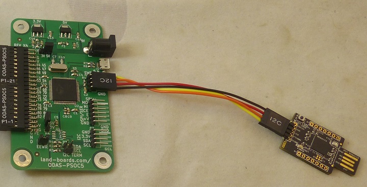
- Programmed using KitProg
- KitProg is a part of CY8CKIT-059
- Has a CY8C5868LTI-LP039 used as the programmer
- Fitted with 1x4 right angle header
- VTARG not connected
- Cables
- 4 pin 1:1 Dupont Programming cable
- Plugs into SWD (H1) connector on UUT
- Other end plugs into KitProg J7
- USB A Male to female cable
- 4 pin 1:1 Dupont Programming cable
- CY8CKIT-059 Guide
- KitProg User Manual
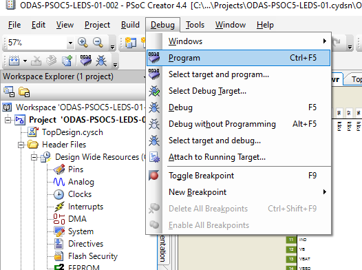
- Program using PSOC Creator
- Select Debug, Program
- Select Device/connect
Factory Acceptance Test (FAT)
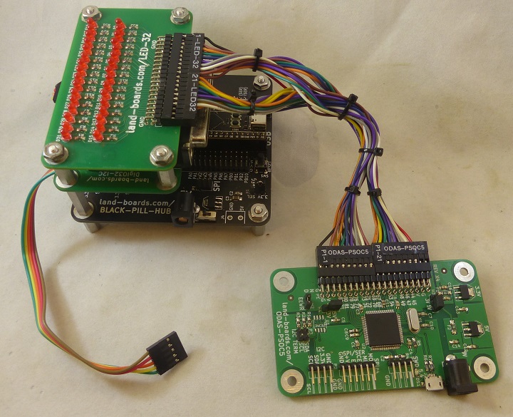
- Unit Under Test (UUT)
- H3 and H4 set to 5V
- P3 SDA, SCL termination jumpers installed
- H2 EEWR jumper installed
- 9V into the DC power jack
- Uses LED-32 card from Arduino Based Test Station
- Cable set from UUT to LED-32
- Running ODAS-PSOC5-LED-01 Build
- Lights are lit in the following order
- D0 through D14, LED on card, then D30 through D17
- D16 = power (always on)
- D15, D31 are not used
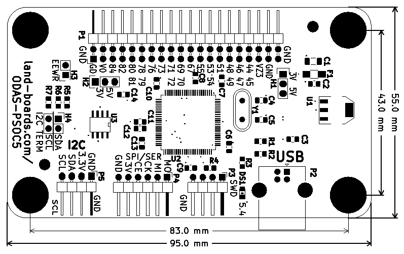
Mechanicals
Software
References
- AN77759 Getting Started with PSoC 5LP
- AN61290 PSoC 5LP Hardware Design Considerations
- AN58304 PSoC 5LP – Pin Selection for Analog Designs
- AN81623 PSoC 5LP Digital Design Best Practices
- AN69133 PSoC 5LP Easy Waveform Generation with the WaveDAC8 Component
- I2C EEPROM example
Revisions
Rev 5
- Change to USB B connector
- Power card from 5V through USB B connector
- Remove 5V regulator
- Re-sequence reference designators top to bottom

