Difference between revisions of "RasPi-GVS"
Blwikiadmin (talk | contribs) |
Blwikiadmin (talk | contribs) |
||
| Line 44: | Line 44: | ||
==== Voltage Translators Architecture ==== | ==== Voltage Translators Architecture ==== | ||
| − | Datasheet | + | [http://www.ti.com/lit/ds/symlink/txs0108e.pdf Datasheet] |
The TXS0108E can be used in level-translation applications for interfacing devices or systems operating at different interface voltages with one another. The TXS0108E is ideal for use in applications where an open-drain driver is connected to the data I/Os. The TXS0108E can also be used in applications where a push-pull driver is connected to the data I/Os, but the TXB0104 might be a better option for such push-pull applications. The TXS0108E device is a semi-buffered auto-direction-sensing voltage translator design is optimized for translation applications (e.g. MMC Card Interfaces) that require the system to start out in a low-speed open-drain mode and then switch to a higher speed push-pull mode. | The TXS0108E can be used in level-translation applications for interfacing devices or systems operating at different interface voltages with one another. The TXS0108E is ideal for use in applications where an open-drain driver is connected to the data I/Os. The TXS0108E can also be used in applications where a push-pull driver is connected to the data I/Os, but the TXB0104 might be a better option for such push-pull applications. The TXS0108E device is a semi-buffered auto-direction-sensing voltage translator design is optimized for translation applications (e.g. MMC Card Interfaces) that require the system to start out in a low-speed open-drain mode and then switch to a higher speed push-pull mode. | ||
| − | TXS0108Arch.PNG | + | [[File:TXS0108Arch.PNG]] |
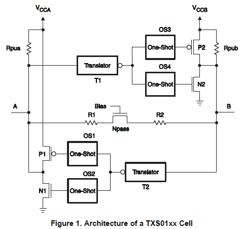
To address these application requirements, a semi-buffered architecture design is used and is illustrated above (see Figure 1). Edge-rate accelerator circuitry (for both the high-to-low and low-to-high edges), a High-Ron n-channel pass-gate transistor (on the order of 300 Ω to 500 Ω) and pull-up resistors (to provide DC-bias and drive capabilities) are included to realize this solution. A direction-control signal (to control the direction of data flow from A to B or from B to A) is not needed. The resulting implementation supports both low-speed open-drain operation as well as high-speed push-pull operation. | To address these application requirements, a semi-buffered architecture design is used and is illustrated above (see Figure 1). Edge-rate accelerator circuitry (for both the high-to-low and low-to-high edges), a High-Ron n-channel pass-gate transistor (on the order of 300 Ω to 500 Ω) and pull-up resistors (to provide DC-bias and drive capabilities) are included to realize this solution. A direction-control signal (to control the direction of data flow from A to B or from B to A) is not needed. The resulting implementation supports both low-speed open-drain operation as well as high-speed push-pull operation. | ||
Revision as of 13:39, 24 January 2020
Contents
Features
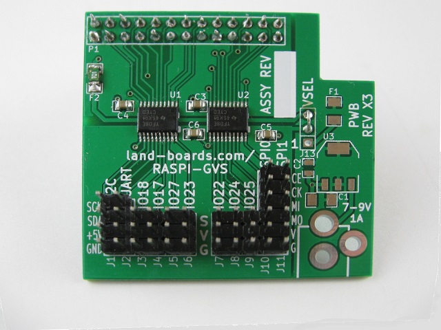
- Daughtercard to the Raspberry Pi (you supply the Raspberry Pi)
- 3.3V to 5V bidirectional voltage translators on GPIO (General Purpose Input/Output) lines
- (7) 5V GPIO lines on GVS connectors
- (2) 5V SPI interfaces (can be used as 5 GPIO lines)
- (1) 5V UART (serial port) interface
- (1) 5V I2C interface (can be used as 2 GPIO lines)
- GPIO_4 enables/disables the voltage translators
- Resettable Fuse protection on the 5V power lines
- 7-9V input voltage on the Power Supply connector (option) which has a regulator that can power the GVS connectors (within thermal limits of the regulator) removing any 5V load from the Raspberry Pi itself
- Jumper to select power for GVS (allows the GVS connectors to be powered from either the on-board regulator (option) or powered from the Raspberry Pi)
- 49x49mm card form factor
Voltage Translators
The Raspi-GVS board uses Texas Instrument TXS0108 voltage translators.
Voltage Translators Features
- No Direction-Control Signal Needed
- Max Data Rates
- 60 Mbps (Push Pull)
- 2 Mbps (Open Drain)
- 1.2 V to 3.6 V on A Port and 1.65 V to 5.5 V on
- B Port (VCCA ≤ VCCB)
- No Power-Supply Sequencing Required –
- Either VCCA or VCCB Can Be Ramped First
- Latch-Up Performance Exceeds 100 mA Per JESD 78, Class II
- ESD Protection Exceeds JESD 22 (A Port)
- 2000-V Human-Body Model (A114-B)
- 150-V Machine Model (A115-A)
- 1000-V Charged-Device Model (C101)
- IEC 61000-4-2 ESD (B Port)
- ±6-kV Air-Gap Discharge
- ±8-kV Contact Discharge
Voltage Translators Architecture
The TXS0108E can be used in level-translation applications for interfacing devices or systems operating at different interface voltages with one another. The TXS0108E is ideal for use in applications where an open-drain driver is connected to the data I/Os. The TXS0108E can also be used in applications where a push-pull driver is connected to the data I/Os, but the TXB0104 might be a better option for such push-pull applications. The TXS0108E device is a semi-buffered auto-direction-sensing voltage translator design is optimized for translation applications (e.g. MMC Card Interfaces) that require the system to start out in a low-speed open-drain mode and then switch to a higher speed push-pull mode.
To address these application requirements, a semi-buffered architecture design is used and is illustrated above (see Figure 1). Edge-rate accelerator circuitry (for both the high-to-low and low-to-high edges), a High-Ron n-channel pass-gate transistor (on the order of 300 Ω to 500 Ω) and pull-up resistors (to provide DC-bias and drive capabilities) are included to realize this solution. A direction-control signal (to control the direction of data flow from A to B or from B to A) is not needed. The resulting implementation supports both low-speed open-drain operation as well as high-speed push-pull operation.
When transmitting data from A to B ports, during a rising edge the One-Shot (OS3) turns on the PMOS transistor (P2) for a short-duration and this speeds up the low-to-high transition. Similarly, during a falling edge, when transmitting data from A to B, the One-Shot (OS4) turns on NMOS transistor (N2) for a short-duration and this speeds up the high-to-low transition. The B-port edge-rate accelerator consists of one-shots OS3 and OS4, Transistors P2 and N2 and serves to rapidly force the B port high or low when a corresponding transition is detected on the A port.
When transmitting data from B to A ports, during a rising edge the One-Shot (OS1) turns on the PMOS transistor (P1) for a short-duration and this speeds up the low-to-high transition. Similarly, during a falling edge, when transmitting data from B to A, the One-Shot (OS2) turns on NMOS transistor (N1) for a short-duration and this speeds up the high-to-low transition. The A-port edge-rate accelerator consists of one-shots OS1 and OS2, Transistors P1 and N1 components and form the edge-rate accelerator and serves to rapidly force the A port high or low when a corresponding transition is detected on the B port.
Power Supply The RaspPi-GVS offers flexible power supply options. The 5V for the GVS Connnectors and translators can come either from the Raspberry Pi or from the 5V power supply on the RaspPi-GVS.
A three pin header and jumpers are used to select the voltage source(s). Installing a single jumper from pins 2 to 3 allow the Raspberry Pi to power the GVC connectors and voltage translators. Installing a jumper from 1 to 2 powers the GVS connections and voltage translators from the 5V power supply.


