Difference between revisions of "KiCad"
Jump to navigation
Jump to search
Blwikiadmin (talk | contribs) |
Blwikiadmin (talk | contribs) |
||
| (41 intermediate revisions by the same user not shown) | |||
| Line 1: | Line 1: | ||
| + | == Locate JLC Order number on PCB == | ||
| + | |||
| + | * To indicate the location, simply add the text "JLCJLCJLCJLC" to the silk layer and select the '''"Specify a location"''' option when placing your order. | ||
| + | * Please note that if this option is not chosen, we may not notice that you have added the text. | ||
| + | * Note: Use only "JLCJLCJLCJLC" without any additional characters. | ||
| + | * The font size should be larger than 0.8mm in height and 0.15mm in width. | ||
| + | |||
== Notes on Running KiCad == | == Notes on Running KiCad == | ||
| Line 4: | Line 11: | ||
== Custom BOM Python Script (KiCad 6) == | == Custom BOM Python Script (KiCad 6) == | ||
| − | |||
| − | |||
* Create a BOM that requires minimal manual editing to use on MediaWiki webpage | * Create a BOM that requires minimal manual editing to use on MediaWiki webpage | ||
| Line 13: | Line 18: | ||
=== Source Code === | === Source Code === | ||
| + | * [https://github.com/openscopeproject/InteractiveHtmlBom/wiki/Installation InteractiveHtmlBom GitHub page] | ||
* [https://github.com/land-boards/lb-boards/blob/master/KiCAD/pyScripts/LandBoardsBOM.py LandBoardsBOM.py] - our BOM script that runs from "Generate Bill of Materials..." in KiCad Schematic Editor | * [https://github.com/land-boards/lb-boards/blob/master/KiCAD/pyScripts/LandBoardsBOM.py LandBoardsBOM.py] - our BOM script that runs from "Generate Bill of Materials..." in KiCad Schematic Editor | ||
** Based on com_csv_grouped_by_value.py that comes in KiCad 6 | ** Based on com_csv_grouped_by_value.py that comes in KiCad 6 | ||
| Line 40: | Line 46: | ||
* Edit in spreadsheet program | * Edit in spreadsheet program | ||
* Use [https://github.com/land-boards/lb-Python-Code/tree/master/pyCSVtoMWTable/src pyCSVtoMWTable] to create MediaWiki format output | * Use [https://github.com/land-boards/lb-Python-Code/tree/master/pyCSVtoMWTable/src pyCSVtoMWTable] to create MediaWiki format output | ||
| + | |||
| + | == Interactive BOM == | ||
| + | |||
| + | * [https://github.com/openscopeproject/InteractiveHtmlBom/wiki/Installation Interactive BOM Installation] | ||
| + | |||
| + | [[file:InteractiveBOM.PNG]] | ||
== Panelizing == | == Panelizing == | ||
| Line 46: | Line 58: | ||
** [https://github.com/ThisIsNotRocketScience/GerberTools/tree/master/GerberPanelizer GerberPanelizer] | ** [https://github.com/ThisIsNotRocketScience/GerberTools/tree/master/GerberPanelizer GerberPanelizer] | ||
** [https://github.com/ThisIsNotRocketScience/GerberTools GerberTools] | ** [https://github.com/ThisIsNotRocketScience/GerberTools GerberTools] | ||
| + | |||
| + | === GerberPanelizer Steps in KiCad 6 === | ||
| + | |||
| + | * Much easier to use Panel by JLCPCB | ||
| + | ** Boards nicely V-Cut/scored | ||
| + | |||
| + | <video type="youtube">qObgLdb5MU4</video> | ||
| + | |||
| + | * Make card | ||
| + | * Run/resolve all DRCs in PCB | ||
| + | * Set Place > Grid Origin to upper left corner of board | ||
| + | * Gerbers | ||
| + | ** Use auxiliary axis as origin | ||
| + | ** Protel extensions | ||
| + | |||
| + | [[file:Panelize_Gerber.PNG]] | ||
| + | |||
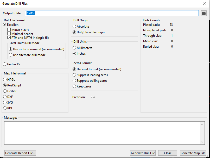
| + | * Save Drill file | ||
| + | |||
| + | [[file:Panelize_Drill.PNG]] | ||
| + | |||
| + | * Rename EdgeCuts .gm1 file to .gko | ||
| + | * Run GerberPanelizer | ||
| + | * File > New | ||
| + | * Select board placement → add gerber folder | ||
| + | ** File browser is painful (can't easily browse) | ||
| + | *** Library > Documents > GitHub > land-boards > lb-boards > folder_with_gerbers | ||
| + | * Board Placement > Autopack: Naive | ||
| + | * Select Board instance in upper right box | ||
| + | |||
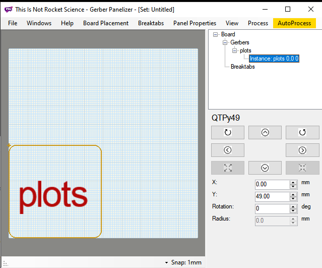
| + | [[file:Panelize_Select_Board_Instance.PNG]] | ||
| + | |||
| + | * Right click, Add instance | ||
| + | ** Repeat for all boards | ||
| + | * Board Placement > Autopack: Naive | ||
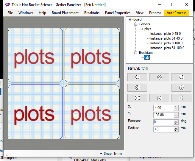
| + | * Breaktabs < Insert Breaktab | ||
| + | |||
| + | [[file:Panelize_Breaktabs_Offset.PNG]] | ||
| + | |||
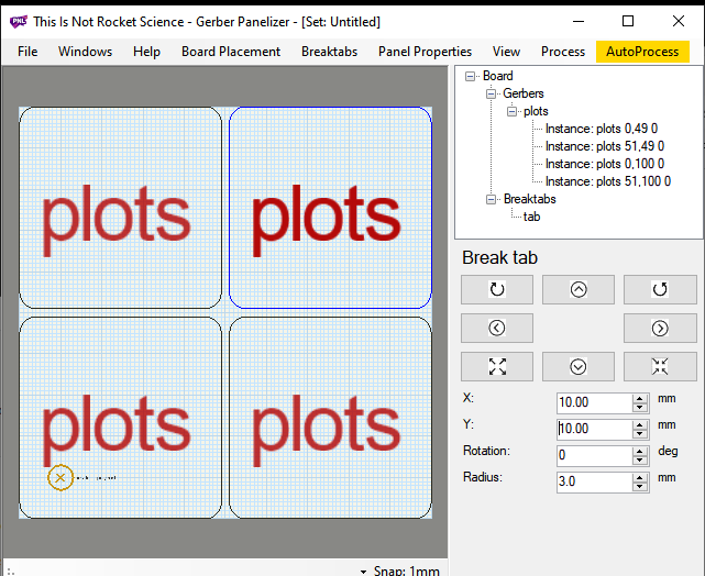
| + | * If not visible, change numbers to 10, 10 | ||
| + | |||
| + | [[file:Panelize_Breaktabs_10-10.PNG]] | ||
| + | |||
| + | * Manually move to spot | ||
| + | * Repeat until cards are all green | ||
| + | |||
| + | [[file:Panelize_Breaktabs_AllGreen.PNG]] | ||
| + | |||
| + | * file → save as to panel folder | ||
| + | * file → export merged file | ||
| + | ** Painful browser to planelized folder | ||
| + | * Make zip | ||
| + | |||
| + | [[file:Panelize_Breaktabs_FinalZIP.PNG]] | ||
| + | |||
| + | * Ordering on jlcpcb | ||
| + | ** Upload file | ||
| + | * Select qty, color | ||
| + | * Select panel by customer | ||
| + | * Enter array dimensions | ||
| + | * Ignore error? | ||
| + | * Not cost goes from $5 to $12.30 for qty 10 | ||
| + | |||
| + | [[file:Panelize_Order_jlcpcb.PNG]] | ||
| + | |||
| + | == JLCPCB Lot Number == | ||
| + | |||
| + | * The location of the [https://support.jlcpcb.com/article/28-how-to-remove-order-number-from-your-pcb JLCPCB Lot Number can be manually placed] | ||
| + | * You can indicate this location by adding the text of " JLCJLCJLCJLC" to silk layer, and select the "Specify a location" option when you place an order. If this option hasn't been chosen, we may not notice you've added the text. | ||
| + | Note: Just "JLCJLCJLCJLC", No more or less characters. The font size should be larger than 0.8mm in height and 0.15 mm in width. | ||
| + | * If you choose Panel by JLCPCB option when you place your order, then we will add the order number on the tooling strip by default, so there is no serial number on your product PCB. | ||
== SPICE Simulation == | == SPICE Simulation == | ||
| Line 52: | Line 135: | ||
== Create Footprints Using FreeCAD == | == Create Footprints Using FreeCAD == | ||
| + | |||
| + | * Our very simple example | ||
<video type="youtube">SabWe5iBN90</video> | <video type="youtube">SabWe5iBN90</video> | ||
== "Standard" Footprints == | == "Standard" Footprints == | ||
| + | |||
| + | * KiCad footprints can be a pain so this documents the footprints we commonly use | ||
=== 1/8 W resistor footprint === | === 1/8 W resistor footprint === | ||
| Line 68: | Line 155: | ||
Resistor_THT:R_Axial_DIN0204_L3.6mm_D1.6mm_P7.62mm_Horizontal | Resistor_THT:R_Axial_DIN0204_L3.6mm_D1.6mm_P7.62mm_Horizontal | ||
</pre> | </pre> | ||
| + | |||
| + | * Also fits 1/4W resistors with leads bent straight down | ||
| + | |||
| + | [[file:Res_8th_Qrtr_W_P18205.JPG]] | ||
=== 1/4 W resistor footprint === | === 1/4 W resistor footprint === | ||
| Line 93: | Line 184: | ||
</pre> | </pre> | ||
| − | * | + | === ZIF Socket === |
| + | |||
| + | * Big rectangular pins | ||
| + | * Too big for "standard" DIP holes | ||
| + | * A lot of pushing can get the socket | ||
| + | * Squeezable pins vertically | ||
| + | * Measures at 0.033" wide, 0.017" tall | ||
| + | * Standard plated hole 0.0315" (0.8mm) | ||
| + | * Make hole oval | ||
| + | ** 1.2mm x 8mm (0.047" x 0.033") | ||
| + | |||
| + | == D-Sub Connectors == | ||
| + | |||
| + | === DB-25F === | ||
| + | |||
| + | * [https://www.mouser.com/ProductDetail/649-D25S33E4PA00LF D25S33E4PA00LF] - DB-25F | ||
| + | ** [https://www.amphenol-cs.com/media/wysiwyg/files/documentation/datasheet/inputoutput/io_dsub_standard_board_mount.pdf Datasheet] | ||
| + | |||
| + | [[FILE:DB25F_DATASHEET.PNG]] | ||
| + | |||
| + | * 3D part | ||
| + | ** '''${KICAD6_3DMODEL_DIR}/Connector_Dsub.3dshapes/DSUB-25_Female_Horizontal_P2.77x2.84mm_EdgePinOffset7.70mm_Housed_MountingHolesOffset9.12mm.wrl''' | ||
| + | |||
| + | [[FILE:DB25F_3D.PNG]] | ||
| − | + | * PCB Footprint | |
| − | + | ** LandBoards_Conns:DB25FC_Oval_Pads | |
| − | + | ||
| + | [[FILE:DB25F_footprint.PNG]] | ||
| + | |||
| + | == Board Design Templates == | ||
| + | |||
| + | * KiCad Templates for | ||
| + | ** BeagleBone Black Capes | ||
| + | ** ODAS 49mm Cards | ||
| + | ** ODAS 95mm Cards | ||
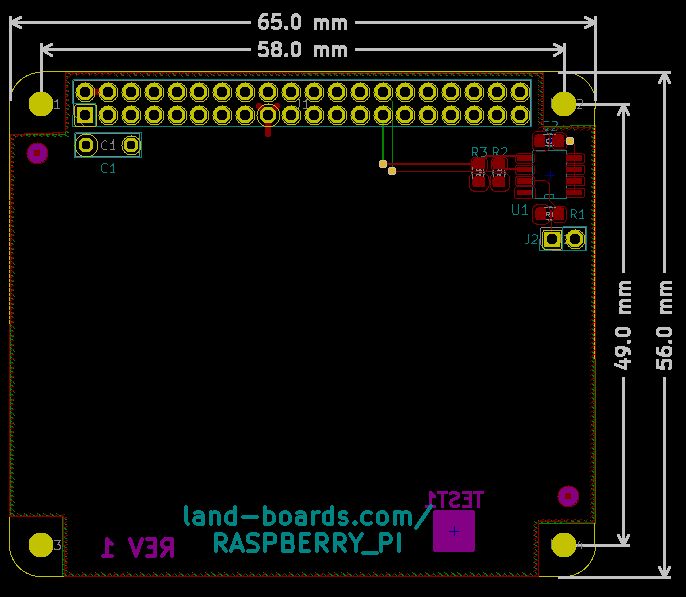
| + | ** Raspberry Pi Plus Hats | ||
| + | * [https://github.com/land-boards/lb-boards/tree/master/KiCAD/templates Templates Repository] | ||
| + | ** ZIP files of each template inside each folder | ||
| + | |||
| + | === BeagleBone Black Cape Template === | ||
| + | |||
| + | * [https://github.com/land-boards/lb-boards/tree/master/KiCAD/templates/BeagleBone_Black BeagleBone Black Cape Template Repository] | ||
| + | |||
| + | [[file:BBB_Template_Color_CAD.PNG]] | ||
| + | |||
| + | === ODAS 49mm Card Template === | ||
| + | |||
| + | * [https://github.com/land-boards/lb-boards/tree/master/KiCAD/templates/ODAS_49mm ODAS 49mm Card Template Repository] | ||
| + | |||
| + | [[file:ODAS_49mm_color_CAD.PNG]] | ||
| + | |||
| + | === ODAS 95mm Card Template === | ||
| + | |||
| + | * [https://github.com/land-boards/lb-boards/tree/master/KiCAD/templates/ODAS_95mm ODAS 95mm Card Template Repository] | ||
| + | |||
| + | [[file:ODAS_95mm_Color_CAD.PNG]] | ||
| + | |||
| + | === Raspberry Pi Plus Hat Template === | ||
| + | |||
| + | * [https://github.com/land-boards/lb-boards/tree/master/KiCAD/templates/Raspberry_Pi Raspberry Pi Plus Hat Template Repository] | ||
| + | |||
| + | [[file:Raspberry_Pi_MECHS.PNG]] | ||
Latest revision as of 11:10, 17 September 2024
Contents
Locate JLC Order number on PCB
- To indicate the location, simply add the text "JLCJLCJLCJLC" to the silk layer and select the "Specify a location" option when placing your order.
- Please note that if this option is not chosen, we may not notice that you have added the text.
- Note: Use only "JLCJLCJLCJLC" without any additional characters.
- The font size should be larger than 0.8mm in height and 0.15mm in width.
Notes on Running KiCad
Some misc. stuff
Custom BOM Python Script (KiCad 6)
- Create a BOM that requires minimal manual editing to use on MediaWiki webpage
- Adds Datasheet path to Description
- Creates BOM .csv file in the folder where the schematic is located
Source Code
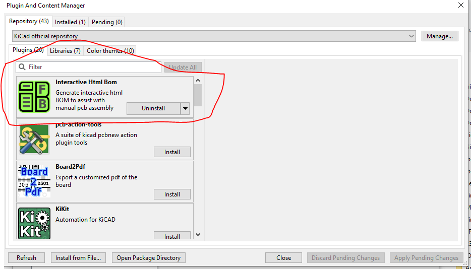
- InteractiveHtmlBom GitHub page
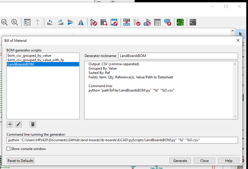
- LandBoardsBOM.py - our BOM script that runs from "Generate Bill of Materials..." in KiCad Schematic Editor
- Based on com_csv_grouped_by_value.py that comes in KiCad 6
- Also requires files from the KiCad installation (get latest from the KiCad installation folder)
- Put the 3 scripts into folder in KiCad projects pyScripts folder
Running
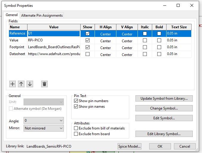
- Add links to schematic parts
- Run BOM tool inside schematic
- Add link to script in KiCad
- Click Generate
Post-Processing
- Edit in spreadsheet program
- Use pyCSVtoMWTable to create MediaWiki format output
Interactive BOM
Panelizing
GerberPanelizer Steps in KiCad 6
- Much easier to use Panel by JLCPCB
- Boards nicely V-Cut/scored
- Make card
- Run/resolve all DRCs in PCB
- Set Place > Grid Origin to upper left corner of board
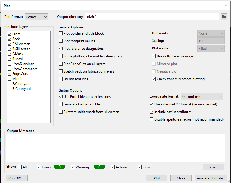
- Gerbers
- Use auxiliary axis as origin
- Protel extensions
- Save Drill file
- Rename EdgeCuts .gm1 file to .gko
- Run GerberPanelizer
- File > New
- Select board placement → add gerber folder
- File browser is painful (can't easily browse)
- Library > Documents > GitHub > land-boards > lb-boards > folder_with_gerbers
- File browser is painful (can't easily browse)
- Board Placement > Autopack: Naive
- Select Board instance in upper right box
- Right click, Add instance
- Repeat for all boards
- Board Placement > Autopack: Naive
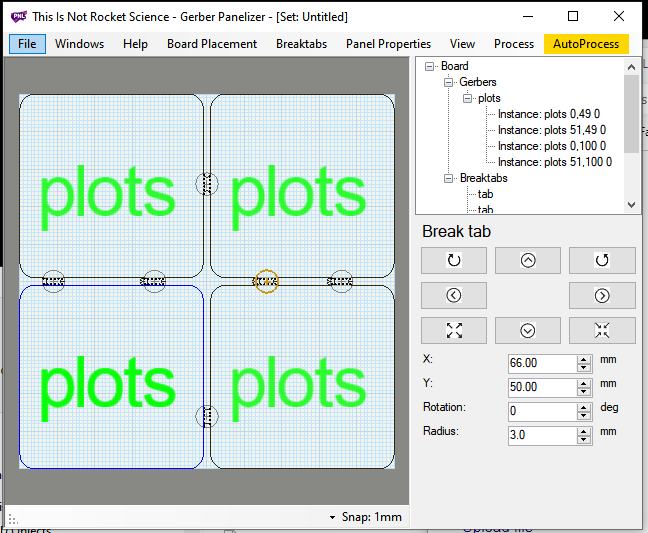
- Breaktabs < Insert Breaktab
- If not visible, change numbers to 10, 10
- Manually move to spot
- Repeat until cards are all green
- file → save as to panel folder
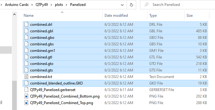
- file → export merged file
- Painful browser to planelized folder
- Make zip
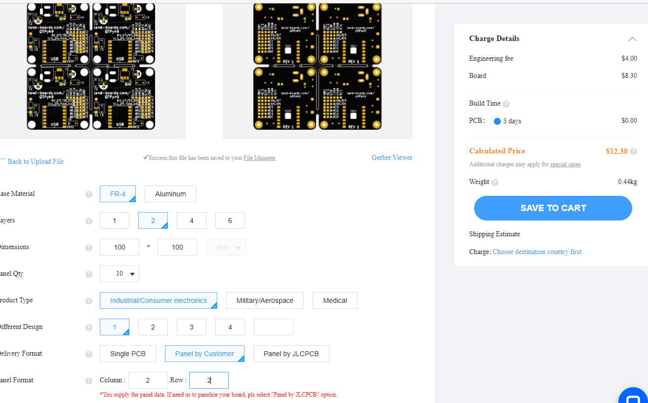
- Ordering on jlcpcb
- Upload file
- Select qty, color
- Select panel by customer
- Enter array dimensions
- Ignore error?
- Not cost goes from $5 to $12.30 for qty 10
JLCPCB Lot Number
- The location of the JLCPCB Lot Number can be manually placed
- You can indicate this location by adding the text of " JLCJLCJLCJLC" to silk layer, and select the "Specify a location" option when you place an order. If this option hasn't been chosen, we may not notice you've added the text.
Note: Just "JLCJLCJLCJLC", No more or less characters. The font size should be larger than 0.8mm in height and 0.15 mm in width.
- If you choose Panel by JLCPCB option when you place your order, then we will add the order number on the tooling strip by default, so there is no serial number on your product PCB.
SPICE Simulation
Create Footprints Using FreeCAD
- Our very simple example
"Standard" Footprints
- KiCad footprints can be a pain so this documents the footprints we commonly use
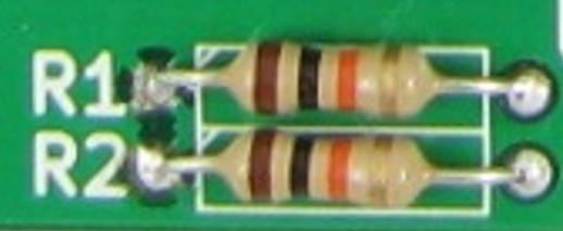
1/8 W resistor footprint
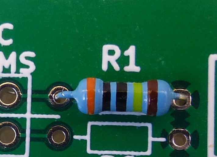
- Part on PCB
- KiCad v6 footprint
Resistor_THT:R_Axial_DIN0204_L3.6mm_D1.6mm_P7.62mm_Horizontal
- Also fits 1/4W resistors with leads bent straight down
1/4 W resistor footprint
- Part on PCB
- KiCad v6 footprint
Resistor_THT:R_Axial_DIN0207_L6.3mm_D2.5mm_P10.16mm_Horizontal
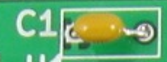
Cap, 0.2" pitch
- Part on PCB
- KiCad v6 footprint
Capacitor_THT:C_Rect_L7.0mm_W3.5mm_P5.00mm
ZIF Socket
- Big rectangular pins
- Too big for "standard" DIP holes
- A lot of pushing can get the socket
- Squeezable pins vertically
- Measures at 0.033" wide, 0.017" tall
- Standard plated hole 0.0315" (0.8mm)
- Make hole oval
- 1.2mm x 8mm (0.047" x 0.033")
D-Sub Connectors
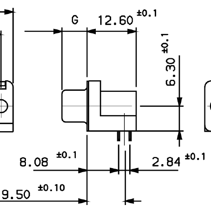
DB-25F
- D25S33E4PA00LF - DB-25F
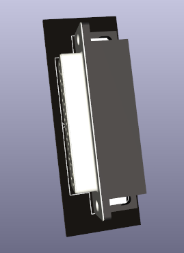
- 3D part
- ${KICAD6_3DMODEL_DIR}/Connector_Dsub.3dshapes/DSUB-25_Female_Horizontal_P2.77x2.84mm_EdgePinOffset7.70mm_Housed_MountingHolesOffset9.12mm.wrl
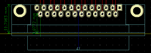
- PCB Footprint
- LandBoards_Conns:DB25FC_Oval_Pads
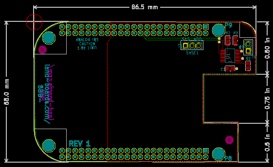
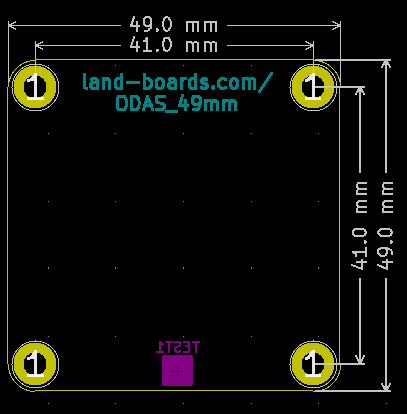
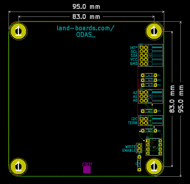
Board Design Templates
- KiCad Templates for
- BeagleBone Black Capes
- ODAS 49mm Cards
- ODAS 95mm Cards
- Raspberry Pi Plus Hats
- Templates Repository
- ZIP files of each template inside each folder
