Difference between revisions of "LB-MEM-02"
Jump to navigation
Jump to search
Blwikiadmin (talk | contribs) |
Blwikiadmin (talk | contribs) |
||
| (55 intermediate revisions by the same user not shown) | |||
| Line 1: | Line 1: | ||
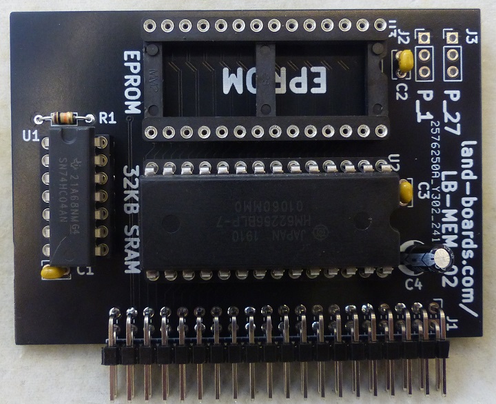
| − | [[file:LB-MEM- | + | [[file:LB-MEM-02_P1090747-720px.jpg]] |
| − | * | + | |
| − | * | + | == Features == |
| − | ** Headers to | + | * 32KB SRAM |
| + | * 16KB EPROM | ||
| + | ** Headers to select PROM bank | ||
* Connects to Address/Data and Memory control lines | * Connects to Address/Data and Memory control lines | ||
* 50x75mm card | * 50x75mm card | ||
| + | |||
| + | == Design == | ||
| + | |||
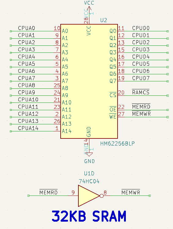
| + | === SRAM === | ||
| + | |||
| + | [[file:LB-MEM-02-SRAM.PNG]] | ||
| + | |||
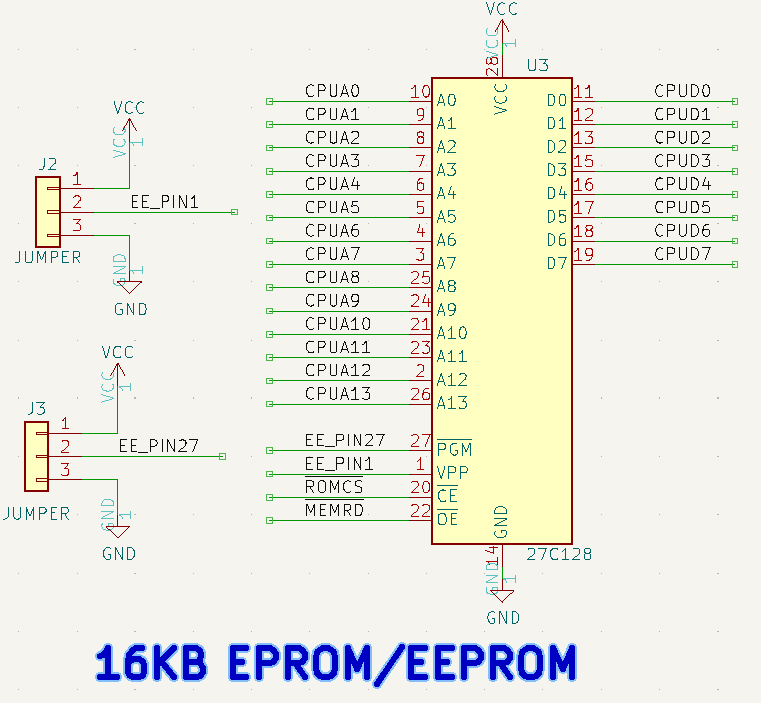
| + | === EPROM === | ||
| + | |||
| + | * ATF16V8B part | ||
| + | * [[TL866ii_Plus_Programmer]] | ||
| + | |||
| + | [[file:LB-MEM-02-PROM.PNG]] | ||
| + | |||
| + | * [[LB-65CXX-01]] card has 16 KB PROM from 0xC000-0xFFFF | ||
| + | * [[LB-6802-01]] card has 16 KB PROM from 0xC000-0xFFFF | ||
| + | * [[LB-6809-01]] card has 16 KB PROM from 0xC000-0xFFFF | ||
| + | * [[LB-Z80-01]] card has 8KB PROM from 0x0000-0x1FFF (upper 8KB is not used) | ||
| + | |||
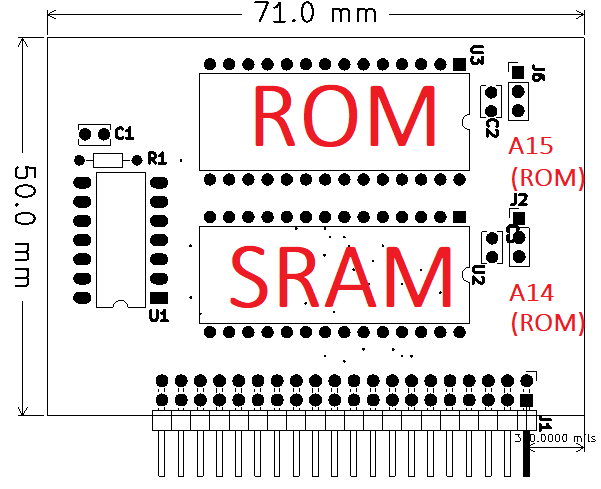
| + | ==== Parts/Jumpers ==== | ||
| + | |||
| + | * Square pin is pin 1 | ||
| + | |||
| + | [[FILE:LB-MEM-02_REV1_MECH_Ann.png]] | ||
| + | |||
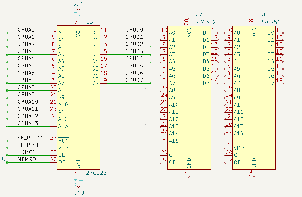
| + | ==== 27C256/27C512 EPROMs ==== | ||
| + | |||
| + | * Card has a 16KB size from the CPU | ||
| + | * 27C256 (32KB) and 27C512 (64KB) Flash EPROMs are commonly available | ||
| + | * Jumpers allow firmware banks to be selected | ||
| + | ** 2 banks in 27C256 | ||
| + | ** 4 banks in 27C512 | ||
| + | |||
| + | {| class="wikitable" | ||
| + | ! EPROM | ||
| + | ! SIZE | ||
| + | ! BANKS | ||
| + | ! J6(A15/Pin1) | ||
| + | ! J2(A14/Pin27) | ||
| + | ! BANK # | ||
| + | ! LOAD OFFSET | ||
| + | |- | ||
| + | | 27C128 | ||
| + | | 16KB | ||
| + | | 1 | ||
| + | | 2-3 (GND) | ||
| + | | 2-3 (GND) | ||
| + | | 1 | ||
| + | | 0x0000 | ||
| + | |- | ||
| + | | 27C256 | ||
| + | | 32KB | ||
| + | | 2 | ||
| + | | 2-3 (GND) | ||
| + | | 1-2 (VCC) | ||
| + | | 1 | ||
| + | | 0x0000 | ||
| + | |- | ||
| + | | 27C256 | ||
| + | | 32KB | ||
| + | | 2 | ||
| + | | 2-3 (GND) | ||
| + | | 2-3 (GND) | ||
| + | | 2 | ||
| + | | 0x4000 | ||
| + | |- | ||
| + | | 27C512 | ||
| + | | 64KB | ||
| + | | 4 | ||
| + | | 2-3 (GND) | ||
| + | | 2-3 (GND) | ||
| + | | 1 | ||
| + | | 0x0000 | ||
| + | |- | ||
| + | | 27C512 | ||
| + | | 64KB | ||
| + | | 4 | ||
| + | | 2-3 (GND) | ||
| + | | 1-2 (VCC) | ||
| + | | 2 | ||
| + | | 0x4000 | ||
| + | |- | ||
| + | | 27C512 | ||
| + | | 64KB | ||
| + | | 4 | ||
| + | | 1-2 (VCC) | ||
| + | | 2-3 (GND) | ||
| + | | 3 | ||
| + | | 0x8000 | ||
| + | |- | ||
| + | | 27C512 | ||
| + | | 64KB | ||
| + | | 4 | ||
| + | | 1-2 (VCC) | ||
| + | | 1-2 (VCC) | ||
| + | | 4 | ||
| + | | 0xC000 | ||
| + | |- | ||
| + | |} | ||
| + | |||
| + | [[file:LB-MEM-02_EPROM_27C128_256_512.png]] | ||
| + | |||
| + | === Backplane Connector === | ||
| + | |||
| + | [[file:LB-MEM-02-BKPL.PNG]] | ||
| + | |||
| + | == Mechanicals == | ||
| + | |||
| + | === Rev 3 === | ||
| + | |||
| + | === Rev 2 === | ||
| + | |||
| + | [[file:LB-MEM-02_Rev2_MECH.PNG]] | ||
| + | |||
| + | === Rev 1 === | ||
| + | |||
| + | [[file:LB-MEM-02_REV1_MECH.PNG]] | ||
| + | |||
| + | == Checkout == | ||
| + | |||
| + | === Rev 3 === | ||
| + | |||
| + | * Adds PWR and GND on U1 (74HC04) | ||
| + | * Adds electrolytic cap footprint | ||
| + | |||
| + | === Rev 2 === | ||
| + | |||
| + | * Flips 74HC04 orientation | ||
| + | * Missing PWR and GND on U1 (74HC04) | ||
| + | * Tested with [[LB-6809-01]] card | ||
| + | ** Works | ||
| + | |||
| + | === Rev 1 === | ||
| + | |||
| + | * Missing PWR and GND on U1 (74HC04) | ||
| + | ** Added PWR and GND wires to nearest pins with PWR and GND | ||
| + | * SRAM passes in TL866 in SRAM test mode | ||
| + | * Test using [https://raw.githubusercontent.com/douggilliland/Retro-Computers/master/6809/LB-6809/ramLoop/ramLoop.asm ramLoop.asm] software | ||
| + | ** [https://raw.githubusercontent.com/douggilliland/Retro-Computers/master/6809/LB-6809/ramLoop/ramLoop.asm ramLoop.asm] code works on [http://6809.uk/ 6809 Emulator] | ||
| + | *** Forcing an error works | ||
| + | ** Check on card without SRAM | ||
| + | *** Controls/data look OK | ||
| + | |||
| + | == Assembly Sheet == | ||
| + | |||
| + | === Rev 3 === | ||
| + | |||
| + | * [https://land-boards.com/LB-MEM-02/LB-MEM-02_Rev3_ibom.html Interactive BOM] | ||
| + | |||
| + | === Rev 1 === | ||
| + | |||
| + | * [https://land-boards.com/LB-MEM-02/LB-MEM-02_Rev1_ibom.html Interactive BOM] | ||
Latest revision as of 13:47, 16 October 2024
Contents
Features
- 32KB SRAM
- 16KB EPROM
- Headers to select PROM bank
- Connects to Address/Data and Memory control lines
- 50x75mm card
Design
SRAM
EPROM
- ATF16V8B part
- TL866ii_Plus_Programmer
- LB-65CXX-01 card has 16 KB PROM from 0xC000-0xFFFF
- LB-6802-01 card has 16 KB PROM from 0xC000-0xFFFF
- LB-6809-01 card has 16 KB PROM from 0xC000-0xFFFF
- LB-Z80-01 card has 8KB PROM from 0x0000-0x1FFF (upper 8KB is not used)
Parts/Jumpers
- Square pin is pin 1
27C256/27C512 EPROMs
- Card has a 16KB size from the CPU
- 27C256 (32KB) and 27C512 (64KB) Flash EPROMs are commonly available
- Jumpers allow firmware banks to be selected
- 2 banks in 27C256
- 4 banks in 27C512
| EPROM | SIZE | BANKS | J6(A15/Pin1) | J2(A14/Pin27) | BANK # | LOAD OFFSET |
|---|---|---|---|---|---|---|
| 27C128 | 16KB | 1 | 2-3 (GND) | 2-3 (GND) | 1 | 0x0000 |
| 27C256 | 32KB | 2 | 2-3 (GND) | 1-2 (VCC) | 1 | 0x0000 |
| 27C256 | 32KB | 2 | 2-3 (GND) | 2-3 (GND) | 2 | 0x4000 |
| 27C512 | 64KB | 4 | 2-3 (GND) | 2-3 (GND) | 1 | 0x0000 |
| 27C512 | 64KB | 4 | 2-3 (GND) | 1-2 (VCC) | 2 | 0x4000 |
| 27C512 | 64KB | 4 | 1-2 (VCC) | 2-3 (GND) | 3 | 0x8000 |
| 27C512 | 64KB | 4 | 1-2 (VCC) | 1-2 (VCC) | 4 | 0xC000 |
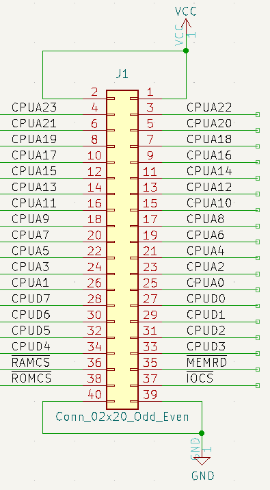
Backplane Connector
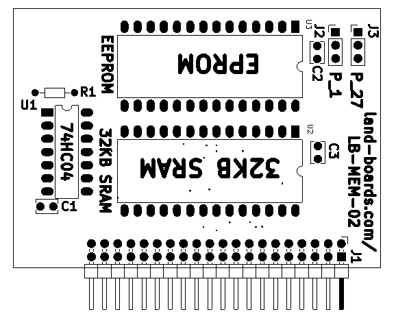
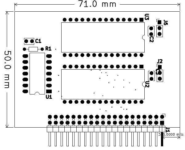
Mechanicals
Rev 3
Rev 2
Rev 1
Checkout
Rev 3
- Adds PWR and GND on U1 (74HC04)
- Adds electrolytic cap footprint
Rev 2
- Flips 74HC04 orientation
- Missing PWR and GND on U1 (74HC04)
- Tested with LB-6809-01 card
- Works
Rev 1
- Missing PWR and GND on U1 (74HC04)
- Added PWR and GND wires to nearest pins with PWR and GND
- SRAM passes in TL866 in SRAM test mode
- Test using ramLoop.asm software
- ramLoop.asm code works on 6809 Emulator
- Forcing an error works
- Check on card without SRAM
- Controls/data look OK
- ramLoop.asm code works on 6809 Emulator
