Difference between revisions of "PDP-11 ON RETRO-EP4CE15"
Jump to navigation
Jump to search
Blwikiadmin (talk | contribs) |
Blwikiadmin (talk | contribs) |
||
| Line 165: | Line 165: | ||
set_location_assignment PIN_K21 -to switch[3] | set_location_assignment PIN_K21 -to switch[3] | ||
set_instance_assignment -name WEAK_PULL_UP_RESISTOR ON -to switch[3] | set_instance_assignment -name WEAK_PULL_UP_RESISTOR ON -to switch[3] | ||
| + | |||
| + | set_location_assignment PIN_AA2 -to ps2k_c | ||
| + | set_location_assignment PIN_AA1 -to ps2k_d | ||
| + | |||
| + | set_location_assignment PIN_A15 -to vgah | ||
| + | set_location_assignment PIN_A14 -to vgav | ||
set_location_assignment PIN_Y9 -to dram_addr[12] | set_location_assignment PIN_Y9 -to dram_addr[12] | ||
| Line 228: | Line 234: | ||
set_location_assignment PIN_N21 -to xu_mosi | set_location_assignment PIN_N21 -to xu_mosi | ||
set_location_assignment PIN_N20 -to xu_sclk | set_location_assignment PIN_N20 -to xu_sclk | ||
| − | |||
| − | |||
| − | |||
| − | |||
| − | |||
</pre> | </pre> | ||
Revision as of 21:02, 27 February 2021
Work in Progress
Contents
Build
- RETRO-EP4CE15
- Requires QM Tech Cyclone V FPGA Board
- Requires EP4CE55 Cyclone IV Card
- PDP2011 by Sytse van Slooten
- David Richards PDP-11 Build on A-ESTF V2 EP4CE22 Board
- System Images
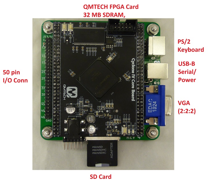
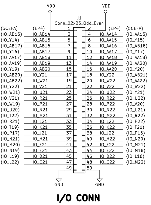
J1 - I/O Connector (5CEFA2F23 FPGA Card pin numbers)
- J1-50 = GND
- J1-49 = GND
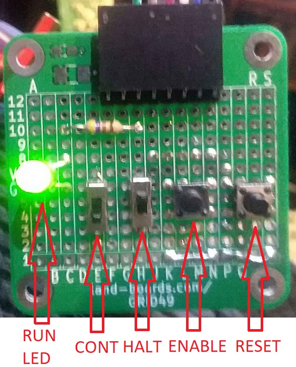
- J1-48 = PIN_M22 = resetbtn
- J1-47 = PIN_L22 = sw_cont
- J1-46 = PIN_L18 = sw_halt
- J1-45 = PIN_L19 = tx2
- J1-44 = PIN_M18 = rx2
- J1-43 = PIN_N19 = rts2
- J1-42 = PIN_M21 = cts2
- J1-41 = PIN_M20 = led_run
- J1-40 = PIN_N20 = xu_sclk
- J1-39 = PIN_N21 = xu_mosi
- J1-38 = PIN_P16 = xu_miso
- J1-37 = PIN_P17 = xu_debug_tx
- J1-36 = PIN_T20 = xu_cs
- J1-35 = PIN_T19 = max7219_load
- J1-34 = PIN_P22 = max7219_data
- J1-33 = PIN_R21 = max7219_clock
- J1-1 = VCC
- J1-2 = VCC
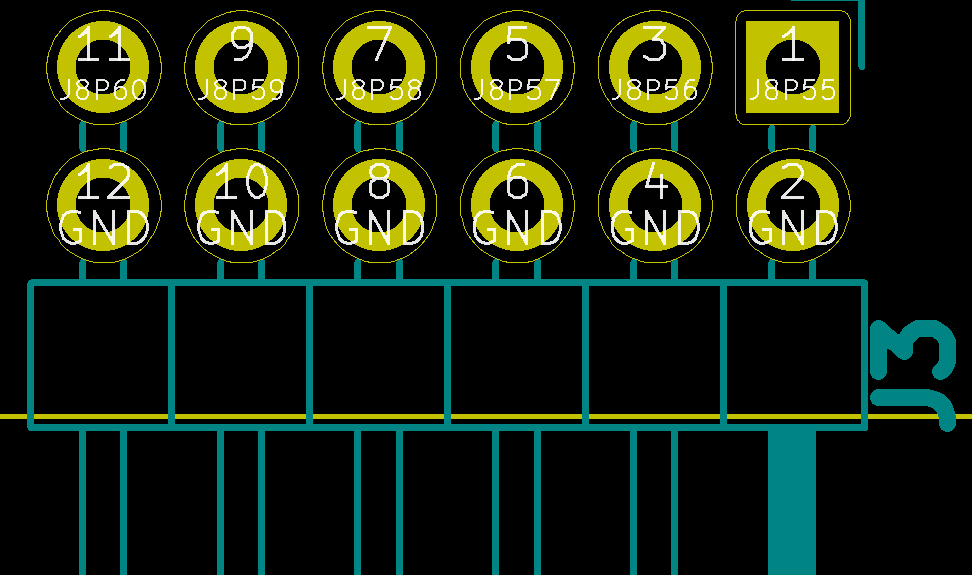
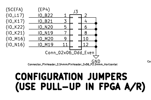
J3 Header (5CEFA2F23 FPGA Card pin numbers)
- J8P55 = PIN_L17
- J8P56 = PIN_K17
- J8B57 = PIN_K22
- J8P58 = PIN_K21
- J8P59 = PIN_M16
- J8P60 = PIN_N16
DIP Switch
| Function | DIP Switch | FPGA Pin |
|---|---|---|
| Swap 0 button | 1 | PIN_M16 |
| treset | 2 | PIN_M15 |
| Swap 2 button | 3 | PIN_B8 |
| Swap console | 4 | PIN_A8 |
Switches
J10 Switches
- Schematic shows J9, Board silkscreen shows J10
| Function | J10 Pin | FPGA Pin |
|---|---|---|
| enablebtn | J10-25 | PIN_J15 |
| resetbtn | J10-27 | PIN_J16 |
| sw_halt | J10-30 | PIN_N14 |
| sw_cont | J10-32 | PIN_P15 |
| led_run | J10-34 | PIN_T15 |
Serial Port
- PIN_T5 = rx1 (in)
- PIN_T6 = tx1 (out)
- PIN_R16 = rx2 (in)
- PIN_P14 = tx2 (out)
- PIN_P16 = rts2 (out)
- PIN_N16 = cts2 (in)
External 8 Digit 7 segment MAX7219 LED
- PIN_L15 max7219_data J10-24
- PIN_N12 max7219_load J10-26
- PIN_N15 max7219_clock J10-28
Resources
- PDP2011 by Sytse van Slooten
- David J Richards - copied and adapted from pdp2011 by Sytse van Slooten
- David Richards PDP-11 Build
- Scott L Baker PDP11-SOC - PDP-11/20 CPU + UART + Timer + I/O Ports coded in VHDL and implemented for the Lattice iCE40-hx8k dev board
- PDP-11 on BitSavers
- w11: PDP 11/70 CPU and SoC - a PDP-11/70 CPU with memory management unit, but without floating point unit,
- Guide to run operating system images on w11a systems
Pin List
# Pin & Location Assignments
# ==========================

set_location_assignment PIN_M9 -to clkin

set_location_assignment PIN_M22 -to resetbtn
set_instance_assignment -name WEAK_PULL_UP_RESISTOR ON -to resetbtn
set_location_assignment PIN_L22 -to sw_cont
set_instance_assignment -name WEAK_PULL_UP_RESISTOR ON -to sw_cont
set_location_assignment PIN_L18 -to sw_halt
set_instance_assignment -name WEAK_PULL_UP_RESISTOR ON -to sw_halt
set_location_assignment PIN_M20 -to led_run

set_location_assignment PIN_L17 -to switch[0]
set_instance_assignment -name WEAK_PULL_UP_RESISTOR ON -to switch[0]
set_location_assignment PIN_K17 -to switch[1]
set_instance_assignment -name WEAK_PULL_UP_RESISTOR ON -to switch[1]
set_location_assignment PIN_K22 -to switch[2]
set_instance_assignment -name WEAK_PULL_UP_RESISTOR ON -to switch[2]
set_location_assignment PIN_K21 -to switch[3]
set_instance_assignment -name WEAK_PULL_UP_RESISTOR ON -to switch[3]

set_location_assignment PIN_AA2 -to ps2k_c
set_location_assignment PIN_AA1 -to ps2k_d

set_location_assignment PIN_A15 -to vgah
set_location_assignment PIN_A14 -to vgav

set_location_assignment PIN_Y9 -to dram_addr[12]
set_location_assignment PIN_T9 -to dram_addr[11]
set_location_assignment PIN_R6 -to dram_addr[10]
set_location_assignment PIN_W8 -to dram_addr[9]
set_location_assignment PIN_T8 -to dram_addr[8]
set_location_assignment PIN_U8 -to dram_addr[7]
set_location_assignment PIN_V6 -to dram_addr[6]
set_location_assignment PIN_U7 -to dram_addr[5]
set_location_assignment PIN_U6 -to dram_addr[4]
set_location_assignment PIN_N6 -to dram_addr[3]
set_location_assignment PIN_N8 -to dram_addr[2]
set_location_assignment PIN_P7 -to dram_addr[1]
set_location_assignment PIN_P8 -to dram_addr[0]
set_location_assignment PIN_P9 -to dram_ba_1
set_location_assignment PIN_T7 -to dram_ba_0
set_location_assignment PIN_AA7 -to dram_cas_n
set_location_assignment PIN_V9 -to dram_cke
set_location_assignment PIN_AB11 -to dram_clk
set_location_assignment PIN_AB5 -to dram_cs_n
set_location_assignment PIN_P12 -to dram_dq[15]
set_location_assignment PIN_R12 -to dram_dq[14]
set_location_assignment PIN_U12 -to dram_dq[13]
set_location_assignment PIN_R11 -to dram_dq[12]
set_location_assignment PIN_R10 -to dram_dq[11]
set_location_assignment PIN_U11 -to dram_dq[10]
set_location_assignment PIN_T10 -to dram_dq[9]
set_location_assignment PIN_U10 -to dram_dq[8]
set_location_assignment PIN_AA8 -to dram_dq[7]
set_location_assignment PIN_AB8 -to dram_dq[6]
set_location_assignment PIN_AA9 -to dram_dq[5]
set_location_assignment PIN_Y10 -to dram_dq[4]
set_location_assignment PIN_AB10 -to dram_dq[3]
set_location_assignment PIN_AA10 -to dram_dq[2]
set_location_assignment PIN_Y11 -to dram_dq[1]
set_location_assignment PIN_AA12 -to dram_dq[0]
set_location_assignment PIN_V10 -to dram_udqm
set_location_assignment PIN_AB7 -to dram_ldqm
set_location_assignment PIN_AB6 -to dram_ras_n
set_location_assignment PIN_W9 -to dram_we_n

set_location_assignment PIN_G10 -to rx1
set_location_assignment PIN_C11 -to tx1

set_location_assignment PIN_L19 -to tx2
set_location_assignment PIN_M18 -to rx2
set_location_assignment PIN_M21 -to cts2
set_location_assignment PIN_N19 -to rts2

set_location_assignment PIN_C16 -to sdcard_sclk
set_location_assignment PIN_B15 -to sdcard_cs
set_location_assignment PIN_B16 -to sdcard_miso
set_location_assignment PIN_C15 -to sdcard_mosi

set_location_assignment PIN_R21 -to max7219_clock
set_location_assignment PIN_P22 -to max7219_data
set_location_assignment PIN_T19 -to max7219_load

set_location_assignment PIN_T20 -to xu_cs
set_location_assignment PIN_P17 -to xu_debug_tx
set_location_assignment PIN_P16 -to xu_miso
set_location_assignment PIN_N21 -to xu_mosi
set_location_assignment PIN_N20 -to xu_sclk
