Difference between revisions of "SSB6 Design"
Jump to navigation
Jump to search
Blwikiadmin (talk | contribs) |
Blwikiadmin (talk | contribs) |
||
| (53 intermediate revisions by the same user not shown) | |||
| Line 1: | Line 1: | ||
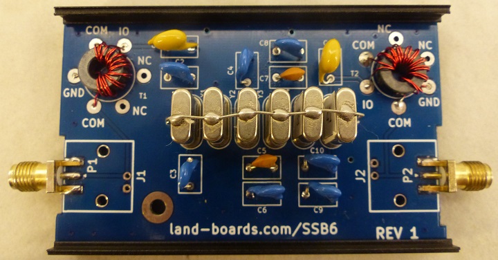
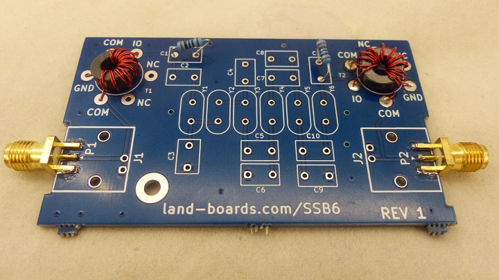
| − | [[FILE: | + | [[FILE:SSB6_P1916-720px.jpg]] |
== Design == | == Design == | ||
| Line 5: | Line 5: | ||
* 6 element filter | * 6 element filter | ||
* [http://w7zoi.net/filters/9megxfils.pdf W7ZOI Crystal Filter paper] has several crystal filter designs | * [http://w7zoi.net/filters/9megxfils.pdf W7ZOI Crystal Filter paper] has several crystal filter designs | ||
| − | * Narrow bandwidth bandpass filters for SSB | + | ** Narrow bandwidth bandpass filters for CW/SSB |
| + | ** This is the 6 crystal SSB6 | ||
* Used for transmit/receive | * Used for transmit/receive | ||
* 9 MHz nominal frequency | * 9 MHz nominal frequency | ||
| Line 35: | Line 36: | ||
[[file:SSB6_SCHEMATIC.PNG]] | [[file:SSB6_SCHEMATIC.PNG]] | ||
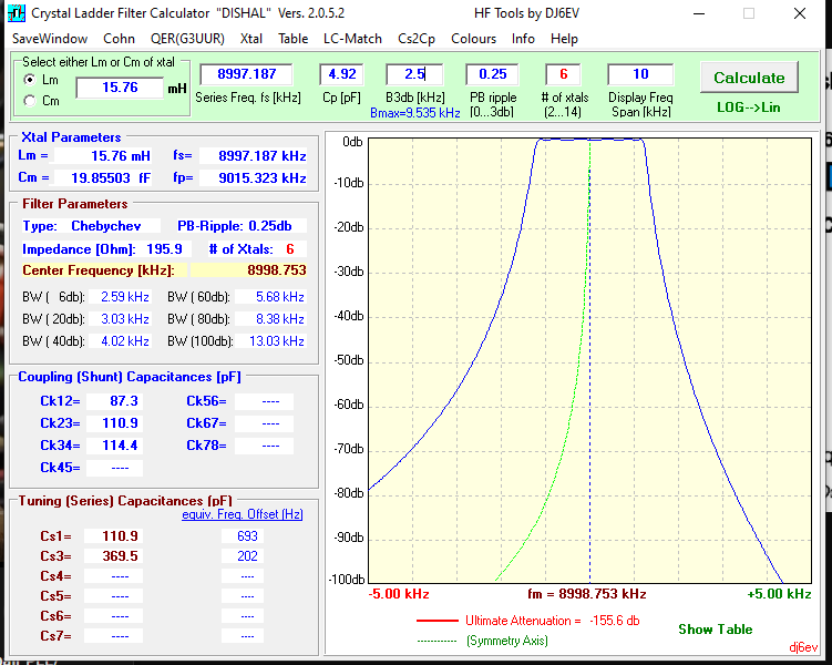
| − | === | + | ==== Dishal Values ==== |
| − | [[ | + | * Impedance = 195.9 |
| + | <pre> | ||
| + | RefDes Dishal RefDes W7ZOI | ||
| + | Ck12 87.3 C3/C9 82 | ||
| + | Ck23 110.9 C4/C8 100 | ||
| + | Ck34 114.4 C6 100 | ||
| + | Cs1 110 C2/C10 120 | ||
| + | Cs3 369.5 C5/C7 470 | ||
| + | </pre> | ||
| + | |||
| + | [[file:Dishal-sim-01.PNG]] | ||
=== Measured Crystal Values === | === Measured Crystal Values === | ||
| + | |||
| + | * 6 crystals within 7 Hz of each other | ||
| + | ** Selected from 50 purchased | ||
<pre> | <pre> | ||
| Line 67: | Line 81: | ||
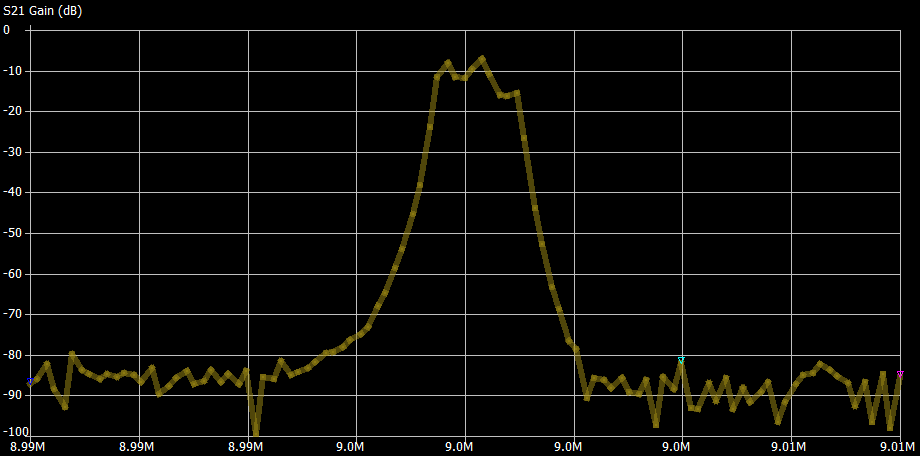
* NanoVNA | * NanoVNA | ||
* 2.5 KHz / div | * 2.5 KHz / div | ||
| + | * Initial measurement shows issues (solved later on this page) | ||
[[file:SSB6_NanoVNA_9MHz_2.5KHzPerDiv.png]] | [[file:SSB6_NanoVNA_9MHz_2.5KHzPerDiv.png]] | ||
| Line 88: | Line 103: | ||
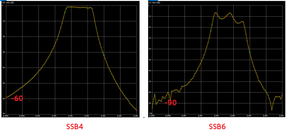
=== Compared to SSB4 === | === Compared to SSB4 === | ||
| − | [[file: | + | * Fcenter = 8.998MHz |
| + | * Span = 10KHz | ||
| + | * 1 KHz/div | ||
| + | * Skirts much deeper on SSB6 than SSB4 | ||
| + | ** -90 dB on SSB6 at window edges | ||
| + | ** -60 dB on SSB4 at window edges | ||
| + | * Passband much flatter on SSB4 | ||
| + | * Insertion loss lower on SSB4 | ||
| + | * SSB4 | ||
| + | |||
| + | [[file:SSB4_vsS_SB6_NanoVNA_9MHz_1KHzPerDiv.png]] | ||
| + | |||
| + | === Improvements === | ||
| + | |||
| + | * Investigate changes to remove ripple and clean up right side of passband | ||
| + | |||
| + | ==== Clean Board ==== | ||
| + | |||
| + | * Cleaned board | ||
| + | * Removed wires on transformer that were not clipped flush-ish | ||
| + | ** No effect - same ripple, same drop at the right side, same insertion loss | ||
| + | * No change | ||
| + | |||
| + | [[file:SB6_NanoVNA_9MHz_1KHzPerDiv_Added_Grounds.png]] | ||
| + | |||
| + | ==== Add grounds to cases of crystals ==== | ||
| + | |||
| + | * Had to scrape away solder mask to solder | ||
| + | ** Through hole vias were plated through | ||
| + | ** Would be better with ground pads with cleared solder mask and thermal relief (Version 2) | ||
| + | * No change | ||
| + | |||
| + | [[file:SSB6_P1889_Soldered-Grounded_Cases_720PX.jpg]] | ||
| + | |||
| + | ==== Incremental Build and Test ==== | ||
| + | |||
| + | * Start with unpopulated board | ||
| + | * Add SMA connectors | ||
| + | |||
| + | [[file:SSB6_P1887_Test_01_SMAs-Installed_720PX.jpg]] | ||
| + | |||
| + | * Added transformers | ||
| + | * Installed 200 ohm resistors at input caps to ground | ||
| + | ** At C1, C11 | ||
| + | |||
| + | [[file:SSB6_P1891_tEST_02_TRANSFORMER_TEST.JPG]] | ||
| + | |||
| + | * Measure transformer impedances from NanoVNA | ||
| + | ** Input | ||
| + | *** 48.9-j0.900 Ohms | ||
| + | *** VSWR 1:1.031 | ||
| + | ** Output | ||
| + | *** 48.7-j0.714 Ohms | ||
| + | *** VSWR 1:1.031 | ||
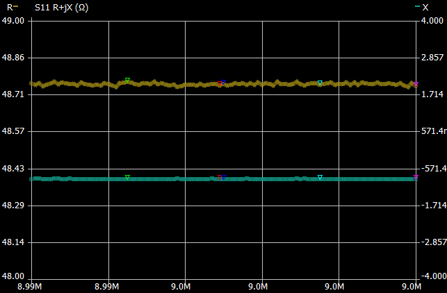
| + | * Impedance is flat over passband | ||
| + | * Transformer working as expected | ||
| + | |||
| + | [[file:SSB6_NanoVNA_9MHz_Transformer_Input_Impedance.png]] | ||
| + | |||
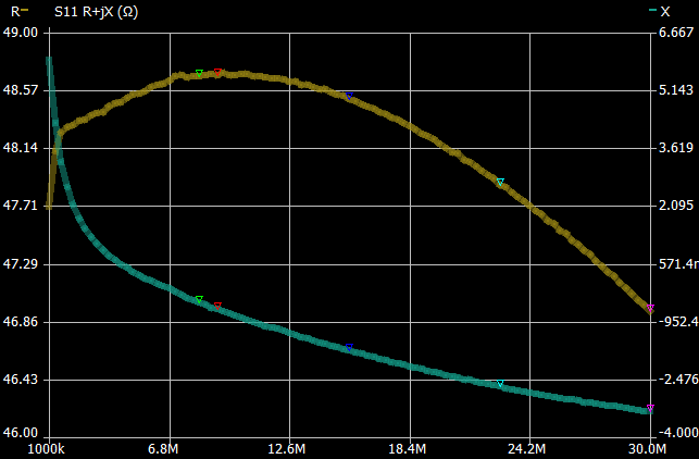
| + | * 1-30 MHz scan | ||
| + | * Toroid flat to board or tilted up = same performance | ||
| + | * Not flat over band, but OK at 9 MHz | ||
| + | |||
| + | [[file:SSB6_NanoVNA_1-30MHz_Transformer_Input_Impedancee.png]] | ||
| + | |||
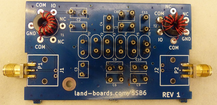
| + | * Add machine socket pins to install parts | ||
| + | |||
| + | [[FILE:SSB6_P1892-720px.jpg]] | ||
| + | |||
| + | * Install caps in socket pins | ||
| + | |||
| + | <pre> | ||
| + | 08 8.997809 10.3 10.3 | ||
| + | 30 8.997810 11.3 11.3 | ||
| + | 48 8.997812 13.3 13.3 | ||
| + | 50 8.997814 15.3 15.3 | ||
| + | 31 8.997818 19.3 19.3 | ||
| + | 46 8.997822 23.3 23.3 | ||
| + | </pre> | ||
| + | |||
| + | * Parts installed on pinned card | ||
| + | |||
| + | [[file:PinJig-01.png]] | ||
| + | |||
| + | ==== Fixed First Card ==== | ||
| + | |||
| + | * Compared pinned board to first board | ||
| + | * Noted C5 and C6 were swapped | ||
| + | * Repaired | ||
| + | * Sweep | ||
| + | |||
| + | [[file:PinJig-02.png]] | ||
| + | |||
| + | * Excellent results | ||
| + | * 2.625KHz bandwidth - close to 2.5KHz design goal | ||
| + | * 2.5 dB insertion loss | ||
| + | * Low ripple. | ||
| + | * Fcenter = 8.998892 MHz | ||
| + | |||
| + | [[file:PinJig-03.png]] | ||
| + | |||
| + | ==== SSB4 vs SSB6 ==== | ||
| + | |||
| + | [[file:SSB4_vsS_SB6_NanoVNA_9MHz_1KHzPerDiv-fixed.png]] | ||
| + | |||
| + | * Input complex impedance across passband | ||
| + | |||
| + | [[ile:SSB6_Input Impedance_InPassband.png]] | ||
== References == | == References == | ||
Latest revision as of 10:59, 30 October 2021
Contents
Design
- 6 element filter
- W7ZOI Crystal Filter paper has several crystal filter designs
- Narrow bandwidth bandpass filters for CW/SSB
- This is the 6 crystal SSB6
- Used for transmit/receive
- 9 MHz nominal frequency
- 50 Ohms in/out impedance
- Bin crystals using Colpitts Crystal Oscillator
- Hand select close values from a pile of crystals
- Can get much closer than 10% of bandwidth with 50 crystals
- W7ZOI Filters on Kits and Parts Boards
- Other filter builds
- 5 or less crystals
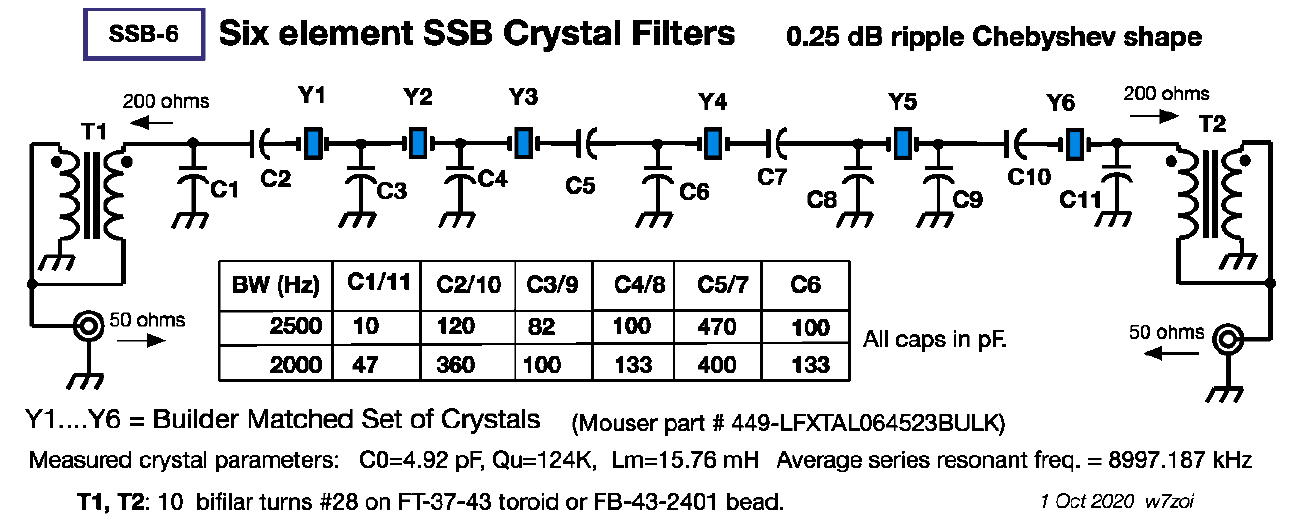
W7ZOI SSB6 Schematic
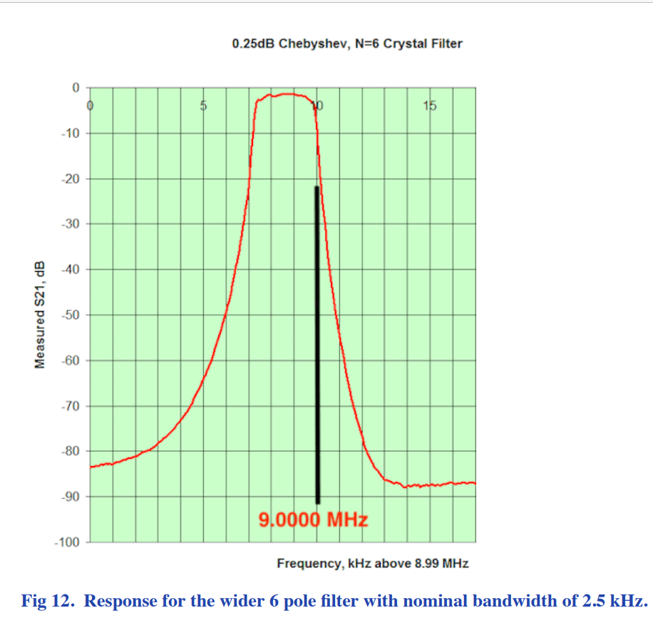
- Response curve
Build
- SSB6 filter is too big for Kits and Parts board (5 crystals limit)
- 2500 Hz bandwidth
Schematic
Dishal Values
- Impedance = 195.9
RefDes Dishal  RefDes W7ZOI
Ck12   87.3    C3/C9  82
Ck23   110.9   C4/C8  100
Ck34   114.4   C6     100
Cs1    110     C2/C10 120
Cs3    369.5   C5/C7  470
Measured Crystal Values
- 6 crystals within 7 Hz of each other
- Selected from 50 purchased
Number Freq        Delta from average
09     8.997791    -7.7
12     8.997791    -7.7
41     8.997793    -5.7
06     8.997794    -4.7
21     8.997798    -0.7
38     8.997798    -0.7
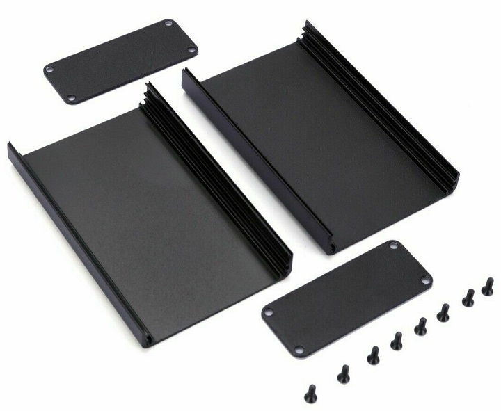
Enclosure 80x50x20
- Fits in 80x50 extruded enclosure
- Material: Aluminum
- Color: black
- Size: approx.80*50*20mm
- Thickness: approx.1mm
Performance Measurements
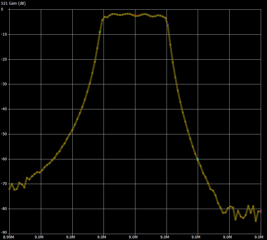
Overall
- NanoVNA
- 2.5 KHz / div
- Initial measurement shows issues (solved later on this page)
Detailed
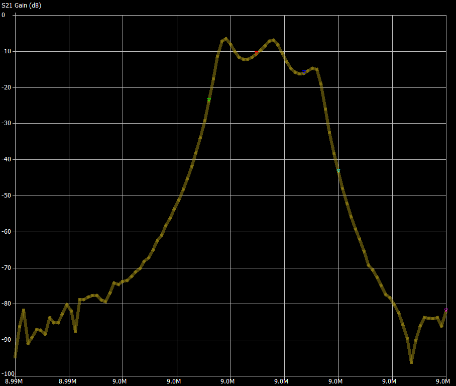
- 1 KHz/div
- Bandpass looks about 2500 KHz = good
- Left freq = 8.99762 MHz
- Right freq = 9.00005 MHz
- Delta = 2.43 KHz
- Center frequency = 8.99885 MHz
- Implies crystals are properly matched?
- Insertion loss at "best" point (red marker) -5.14 dB = OK
- Deep skirts = good
- Ripple looks bad
- Right side low
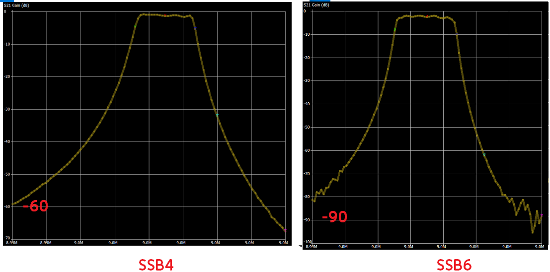
Compared to SSB4
- Fcenter = 8.998MHz
- Span = 10KHz
- 1 KHz/div
- Skirts much deeper on SSB6 than SSB4
- -90 dB on SSB6 at window edges
- -60 dB on SSB4 at window edges
- Passband much flatter on SSB4
- Insertion loss lower on SSB4
- SSB4
Improvements
- Investigate changes to remove ripple and clean up right side of passband
Clean Board
- Cleaned board
- Removed wires on transformer that were not clipped flush-ish
- No effect - same ripple, same drop at the right side, same insertion loss
- No change
Add grounds to cases of crystals
- Had to scrape away solder mask to solder
- Through hole vias were plated through
- Would be better with ground pads with cleared solder mask and thermal relief (Version 2)
- No change
Incremental Build and Test
- Start with unpopulated board
- Add SMA connectors
- Added transformers
- Installed 200 ohm resistors at input caps to ground
- At C1, C11
- Measure transformer impedances from NanoVNA
- Input
- 48.9-j0.900 Ohms
- VSWR 1:1.031
- Output
- 48.7-j0.714 Ohms
- VSWR 1:1.031
- Input
- Impedance is flat over passband
- Transformer working as expected
- 1-30 MHz scan
- Toroid flat to board or tilted up = same performance
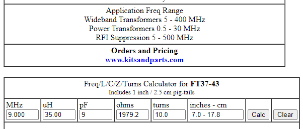
- Not flat over band, but OK at 9 MHz
- Add machine socket pins to install parts
- Install caps in socket pins
08	8.997809	10.3	10.3
30	8.997810	11.3	11.3
48	8.997812	13.3	13.3
50	8.997814	15.3	15.3
31	8.997818	19.3	19.3
46	8.997822	23.3	23.3
- Parts installed on pinned card
Fixed First Card
- Compared pinned board to first board
- Noted C5 and C6 were swapped
- Repaired
- Sweep
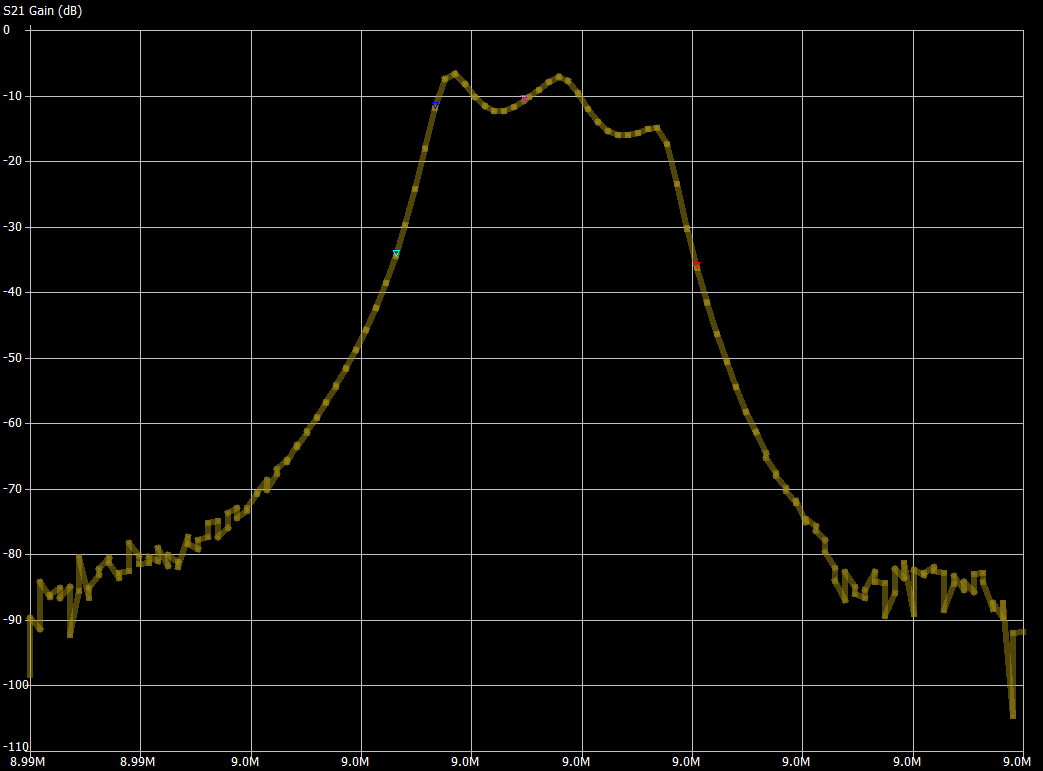
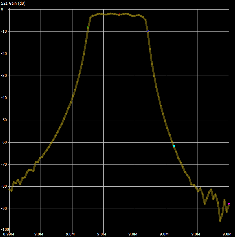
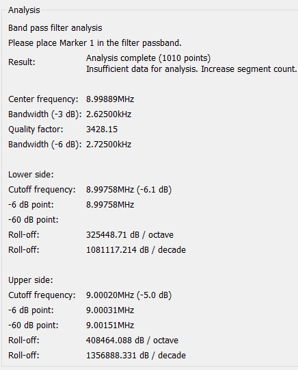
- Excellent results
- 2.625KHz bandwidth - close to 2.5KHz design goal
- 2.5 dB insertion loss
- Low ripple.
- Fcenter = 8.998892 MHz
SSB4 vs SSB6
- Input complex impedance across passband
ile:SSB6_Input Impedance_InPassband.png
References
- Crystal ladder filters – Software
- Crystal Ladder Filters for All - ARRL QEX
- DISHAL software by DJ6EV
- A Practical Test Set for Comprehensive Crystal Testing
- Crystal characterization and crystal filter design
- Crystal parameters Written by Hans Summers (QRP Labs)
