Difference between revisions of "RF-Amp"
Jump to navigation
Jump to search
Blwikiadmin (talk | contribs) |
Blwikiadmin (talk | contribs) |
||
| (165 intermediate revisions by the same user not shown) | |||
| Line 1: | Line 1: | ||
| − | [[File:RF- | + | [[File:RF-Amp_P1943-720px.jpg]] |
== RF Amplifier Features == | == RF Amplifier Features == | ||
| − | * | + | * Class A (Common Emitter) Amplifier |
| − | ** | + | ** Emitter resistor bypassed with capacitor for higher AC gain |
| − | * | + | ** Transformer coupled input/output for impedance matching to 50Ω |
| − | * + | + | ** Capacitively coupled input |
| − | * Input connectors: SMA or | + | * Single 2N3904 NPN transistor |
| + | * Useful as an gain block in various applications | ||
| + | ** Radio Transmitter/Receiver IF Amplifier | ||
| + | ** Radio Transmitter/Receiver Antenna Amplifier | ||
| + | ** Radio Transmitter Microphone amplifier (with minor modifications) | ||
| + | * As RF Amplifier | ||
| + | ** Measured Gain Bandwidth (GBW) of 150 | ||
| + | ** Measured Gain @7 MHz, +25.2 dB at 12V | ||
| + | ** Measured Gain @9 MHz, +24.7 dB at 12V | ||
| + | ** Measured Gain @30 MHz, +13.8 dB at 12V | ||
| + | * As a microphone amplifier | ||
| + | ** Approximately 20 dB at 1 KHz | ||
| + | * Input connectors: SMA, BNC, or direct solder coax to SMA etches | ||
* +12V nominal power | * +12V nominal power | ||
| + | ** 12-14 VDC | ||
| + | ** 5 mm terminal block for power | ||
* 49x49mm card | * 49x49mm card | ||
* 4x 4-40 mounting holes | * 4x 4-40 mounting holes | ||
| + | |||
| + | === Source Materials === | ||
| + | |||
| + | * From [https://zl2ctm.blogspot.com/2020/11/go-qrp-portable-ssb-rig.html Charlie Morris' (ZL2CTM) Go QRP Portable SSB Rig] | ||
| + | ** Charlie references [https://www.amazon.com/Solid-State-Design-Radio-Amateur/dp/0872590402 Solid State Design for the Radio Amateur] (pp 19-20) | ||
| + | |||
| + | === HFE at 10 mA === | ||
| + | |||
| + | [[file:HFE_10mA.PNG]] | ||
== RF Amplifier Design == | == RF Amplifier Design == | ||
| Line 19: | Line 42: | ||
== LT Spice Simulation == | == LT Spice Simulation == | ||
| + | |||
| + | === As Built - Rev 1 === | ||
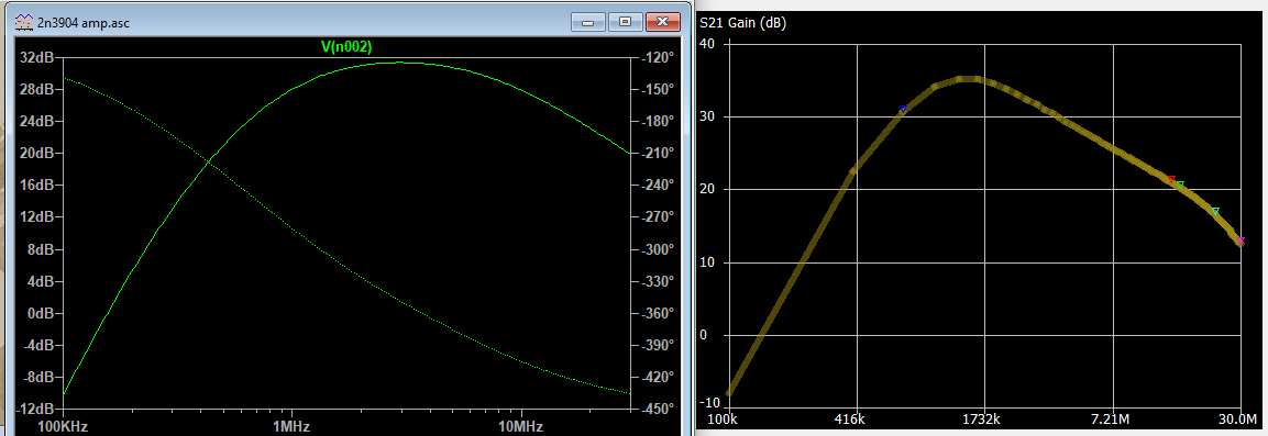
* [https://github.com/land-boards/lb-boards/blob/master/HamRadio/RF-Amp/LTSpice/2n3904%20amp.asc LTspice Simulation] - GitHub source file | * [https://github.com/land-boards/lb-boards/blob/master/HamRadio/RF-Amp/LTSpice/2n3904%20amp.asc LTspice Simulation] - GitHub source file | ||
| Line 25: | Line 50: | ||
[[File:RF-AMP-LTSPICE_XFMRS.PNG]] | [[File:RF-AMP-LTSPICE_XFMRS.PNG]] | ||
| − | == Charlie Morris Design == | + | === Additional Resistor === |
| + | |||
| + | * Insert 4.7 Ω resistor to emitter bypass capacitor | ||
| + | ** Reduces maximum gain | ||
| + | ** Increases gain over 1-30 MHz bandwidth | ||
| + | ** Possible better for Antenna Amplifier application at lower frequencies | ||
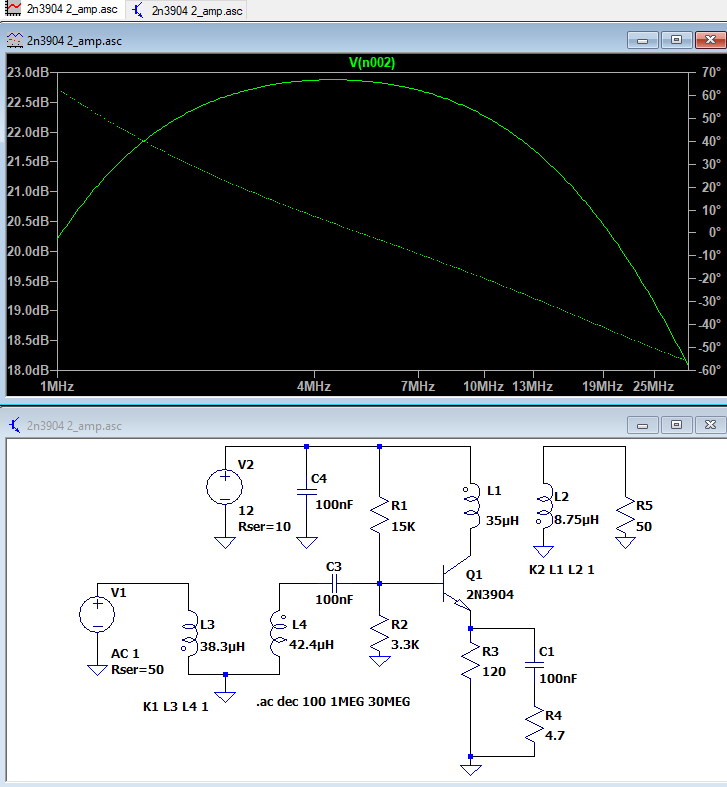
| + | * +22.4 dB at 9 MHz | ||
| + | |||
| + | [[File:RF-AMP-Rev2_LTSPICE.PNG]] | ||
| + | |||
| + | == Charlie Morris Design Calculations == | ||
* From Charlie's notes with mods for my use | * From Charlie's notes with mods for my use | ||
| Line 50: | Line 85: | ||
** If Vce = 6V, this is 60 mW power dissipation | ** If Vce = 6V, this is 60 mW power dissipation | ||
* Assume Ve (voltage across emitter resistor) = 1/10 Vcc = 12V/10 = 1.2V | * Assume Ve (voltage across emitter resistor) = 1/10 Vcc = 12V/10 = 1.2V | ||
| − | ** R3 is Re (emitter resistor) = 1.2V/0.01A = 120 | + | ** R3 is Re (emitter resistor) = 1.2V/0.01A = 120 Ω |
* VCE = 0.7V (typical from data sheet) | * VCE = 0.7V (typical from data sheet) | ||
* V(emitter) at 10% of Vcc rule of thumb = 1.2V | * V(emitter) at 10% of Vcc rule of thumb = 1.2V | ||
| Line 58: | Line 93: | ||
** 10 mA in C-E, beta DC less = 10 mA/173 = 58 uA | ** 10 mA in C-E, beta DC less = 10 mA/173 = 58 uA | ||
** 10x the current in the biasing resistors = 580 uA (calculated) | ** 10x the current in the biasing resistors = 580 uA (calculated) | ||
| − | * R2 is 1.9V at 580 uA = 3. | + | * R2 is 1.9V at 580 uA = 3.29KΩ use 3.3KΩ |
* R1 sources current to R2 and transistor base | * R1 sources current to R2 and transistor base | ||
** Voltage = Vcc (12V) - 1.9V = 10.1V | ** Voltage = Vcc (12V) - 1.9V = 10.1V | ||
** Current = 577 uA + 58 uA = 635 uA | ** Current = 577 uA + 58 uA = 635 uA | ||
| − | ** R1 = 10.1 / .635 mA = 15. | + | ** R1 = 10.1 / .635 mA = 15.9KΩ, use 15KΩ |
==== Measured DC operating point ==== | ==== Measured DC operating point ==== | ||
| Line 69: | Line 104: | ||
* Vcc = 11.96V | * Vcc = 11.96V | ||
* Current draw = 12 mA | * Current draw = 12 mA | ||
| + | ** Quick test for wiring and more or less correct parts | ||
** Expected 11 mA - close enough | ** Expected 11 mA - close enough | ||
* +BUFF = 11.84V | * +BUFF = 11.84V | ||
| − | ** 0.12V which is 12 mA through R4 10 | + | ** 0.12V which is 12 mA through R4 at 10 Ω - expected |
* V emitter = 1.41V | * V emitter = 1.41V | ||
| − | ** | + | ** 1.41V/12Ω = 11.75 mA close to 12 mA total measured current |
* V on input divider = 2.06V | * V on input divider = 2.06V | ||
** Vbase + 0.7V - close | ** Vbase + 0.7V - close | ||
| + | ** Measured Vbe = 2.06-1.41 = 0.65 - close | ||
=== Input resistance === | === Input resistance === | ||
| Line 82: | Line 119: | ||
** C=0.1uF | ** C=0.1uF | ||
** F=10MHz | ** F=10MHz | ||
| − | ** 1/2*pi*F*C = 0. | + | ** 1/2*pi*F*C = 0.16Ω |
* Parallel resistors R1, R2 paralleled with transistor input impedance | * Parallel resistors R1, R2 paralleled with transistor input impedance | ||
| − | ** R1= | + | ** R1=15KΩ, R2=3.3KΩ |
| − | ** Transistor resistance = Beta AC ( | + | ** Transistor resistance = Beta AC (33.3) times re |
*** re = 26 / Ie (10 mA in mA) = 26/10 = 2.6 | *** re = 26 / Ie (10 mA in mA) = 26/10 = 2.6 | ||
*** SSDRA uses 25 as constant - close enough | *** SSDRA uses 25 as constant - close enough | ||
| − | *** Beta AC * re = 33.3*2.6 = 83. | + | **** 26 comes from Ebers-Moll approximation |
| − | ** All in parallel are 80. | + | *** Beta AC * re = 33.3*2.6 = 83.3Ω - predominates |
| + | ** All in parallel are 80.8Ω | ||
| + | |||
| + | === Gain calculation === | ||
| + | |||
| + | * Approximation | ||
| + | * Ic = 0.01A | ||
| + | * Rc = 200 | ||
| + | * Vrc = 2V | ||
| + | * Gain = Vrc / vt | ||
| + | ** vt = 26 mV at room temperature | ||
| + | ** Gain = 2V / .026V = 79.2 V/V | ||
| + | ** Gain = +37 dB | ||
=== Input/Output Transformers === | === Input/Output Transformers === | ||
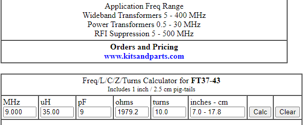
| − | * [http://toroids.info/FT37-43.php FT37-43 Toroid] | + | * Using [http://toroids.info/FT37-43.php FT37-43 Toroid] |
[[file:FT37-43_10_Turns.PNG]] | [[file:FT37-43_10_Turns.PNG]] | ||
| Line 105: | Line 154: | ||
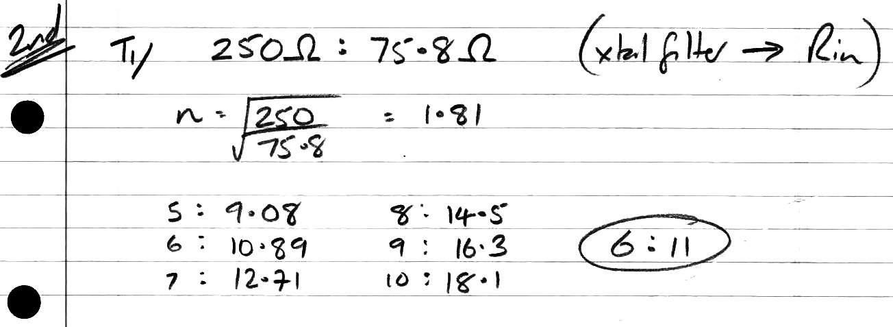
* Input Transformer (T1 on Charlie's - T2 on this board) | * Input Transformer (T1 on Charlie's - T2 on this board) | ||
* Need to calculate turns ratio | * Need to calculate turns ratio | ||
| − | * 50:80.8 | + | * 50:80.8 Ω |
* n = sqrt(Zout/Zin)sqrt(80.8/50) = 1.27 turns ratio | * n = sqrt(Zout/Zin)sqrt(80.8/50) = 1.27 turns ratio | ||
* Turns choices | * Turns choices | ||
* Minimum number of turns | * Minimum number of turns | ||
* Rule of thumb - want Xl (coil impedance smallest value) to be least 4-5X the load | * Rule of thumb - want Xl (coil impedance smallest value) to be least 4-5X the load | ||
| − | ** Load = 80.8 | + | ** Load = 80.8 Ω |
| − | ** 5 * 80.8 | + | ** 5 * 80.8 Ω = 404.2 Ω minimum |
*** More turns = larger capacitance and drops bandwidth | *** More turns = larger capacitance and drops bandwidth | ||
** Toroid is FT37-43 | ** Toroid is FT37-43 | ||
** From [http://toroids.info/FT37-43.php Toroid page] | ** From [http://toroids.info/FT37-43.php Toroid page] | ||
| − | *** Xl = 404. | + | *** Xl = 404.4Ω at 9 MHz is 4.5 turns, round up to 5 |
** Try nearest integer numbers turns ratios | ** Try nearest integer numbers turns ratios | ||
*** 5:6 = 6% error | *** 5:6 = 6% error | ||
| Line 130: | Line 179: | ||
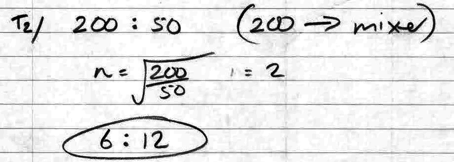
* Output transformer (T2 on Charlie's - T1 on this board) | * Output transformer (T2 on Charlie's - T1 on this board) | ||
| − | * T2 - different than Charlie's design since my Crystal filters are all 50 | + | * T2 - different than Charlie's design since my Crystal filters are all 50 Ω in/out |
| − | * SSDRA suggest presenting 200 | + | * SSDRA suggest presenting 200 Ω load to the collector |
** Can't find reference in SSDRA | ** Can't find reference in SSDRA | ||
| − | ** Reflecting back 50 | + | ** Reflecting back 50 Ω load to 200 Ω collector... |
| − | * 200:50 | + | * 200:50 Ω |
* n = sqrt(200/50) = 2.0:1 turns ratio | * n = sqrt(200/50) = 2.0:1 turns ratio | ||
* 10:5 turns | * 10:5 turns | ||
| Line 141: | Line 190: | ||
** 5 turns secondary (towards output) | ** 5 turns secondary (towards output) | ||
*** 5 turns = 8.75 uH | *** 5 turns = 8.75 uH | ||
| − | * | + | ** 15 turns = 9.5 in |
[[file:RF-Amp-T1.PNG]] | [[file:RF-Amp-T1.PNG]] | ||
| Line 164: | Line 213: | ||
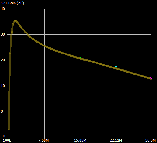
* S21 (gain) needs to be measured with a [[RF_Attenuators#40_dB_Attenuator|40 dB attenuator]] on input to RF-Amp to avoid compression on the output | * S21 (gain) needs to be measured with a [[RF_Attenuators#40_dB_Attenuator|40 dB attenuator]] on input to RF-Amp to avoid compression on the output | ||
* S11 (reflection) input impedance can't be measured with input [[RF_Attenuators#40_dB_Attenuator|40 dB attenuator]] because S11 just ends up measuring the attenuator | * S11 (reflection) input impedance can't be measured with input [[RF_Attenuators#40_dB_Attenuator|40 dB attenuator]] because S11 just ends up measuring the attenuator | ||
| − | ** Output should be terminated to 50 | + | ** Output should be terminated to 50 Ω for S11 measurement |
* DC current = 12 mA | * DC current = 12 mA | ||
| Line 170: | Line 219: | ||
* Put [[RF_Attenuators#40_dB_Attenuator|40 dB attenuator]] on RF-Amp input, measure S21 at output | * Put [[RF_Attenuators#40_dB_Attenuator|40 dB attenuator]] on RF-Amp input, measure S21 at output | ||
| − | ** [[NanoVNA]] provides 50 | + | ** [[NanoVNA]] provides 50 Ω load to RF-Amp to properly terminate output |
* Measure S21 with 9:11 input transformer | * Measure S21 with 9:11 input transformer | ||
** S21 @ 100 KHz = -8 dB dB | ** S21 @ 100 KHz = -8 dB dB | ||
| Line 196: | Line 245: | ||
** Measured output with scope - not clipped at 9 MHz | ** Measured output with scope - not clipped at 9 MHz | ||
*** Approx. 1Vpp input = +22.1 dBm gain which matches the S21 with the attenuator on the input | *** Approx. 1Vpp input = +22.1 dBm gain which matches the S21 with the attenuator on the input | ||
| − | *** Vpp = 12.4V with 50 | + | *** Vpp = 12.4V with 50 Ω load resistor |
** Starts clipping at 7 Mhz and down | ** Starts clipping at 7 Mhz and down | ||
* Therefore, can measure input impedance at 9 MHz | * Therefore, can measure input impedance at 9 MHz | ||
| Line 209: | Line 258: | ||
[[file:RF-Amp_S21_40dBAttenOutput_1-30MHz.png]] | [[file:RF-Amp_S21_40dBAttenOutput_1-30MHz.png]] | ||
| − | === | + | == W2AEW S11 Measurement Method == |
| + | |||
| + | * Can't drive the RF Amp directly from the [[NanoVNA]] | ||
| + | ** High output level from the NanoVNA overdrives the RF Amp | ||
| + | ** W2AEW provides a way of driving the RF Amp card without overdriving and still measure S11 | ||
| + | |||
| + | <video type="youtube">7TtKE39TWpI</video> | ||
| + | |||
| + | * Calibrate NanoVNA using External 30 dB Attenuator | ||
| + | ** See [https://youtu.be/7TtKE39TWpI W2AEW #337 video] above | ||
| + | ** Insert 30 dB attenuator and calibrate with attenuator installed | ||
| + | ** Open/sort/thru at the output side of the attenuator using [[NanoVNA#RF_Demo_Kit|NanoVNA RF Demo Kit]] | ||
| + | *** [[NanoVNA#RF_Demo_Kit|NanoVNA RF Demo Kit]] has similar connectors, etc to RF Amp | ||
| + | * Scan 1-30 Mhz | ||
| + | ** Overdriven at 1 MHz which "swamps" the RF Amp | ||
| + | * Re-calibrated at 1.5-31.5 MHz | ||
| + | ** Peak gain at 1 MHz = 32 dB | ||
| + | *** Does not overdrive the Amp or NanoVNA | ||
| + | *** Downsize is a lot of noise in the return loss | ||
| + | * Tested two units | ||
| + | ** Unit 1 has a 7:10 input transformer (T2) ratio | ||
| + | ** Unit 2 has a 7:9 input transformer (T2) ratio | ||
| + | |||
| + | === Unit 1 === | ||
| + | |||
| + | * 9 MHz measurements | ||
| + | ** VSWR = 1.172 | ||
| + | ** S11 (Return Loss) = -22.014 dB | ||
| + | ** S21 (Gain) = +23.624 dB | ||
| + | |||
| + | [[file:RF-Amp_W2AEW_S21_1-30MHz.png]] | ||
| + | |||
| + | [[file:RF-Amp_W2AEW_S11_1-30MHz.png]] | ||
| + | |||
| + | === Unit 2 === | ||
| + | |||
| + | * 9 MHz measurement | ||
| + | ** VSWR = 1.182 | ||
| + | ** S11 (Return Loss) = -21.565 dB | ||
| + | ** S21 (Gain) = +24.656 dB | ||
| + | * 20 dB gain at 15 MHz | ||
| + | ** Gain Bandwidth (GBW) = ~150 | ||
| + | ** GBW is a good predictor of gain at particular frequencies | ||
| + | ** Calculated Gain of 14 dB at 30 MHz - measured at +12.8 dB | ||
| + | ** Measured at +26 dB at 7 MHz | ||
| + | |||
| + | [[file:RF-Amp_U2_W2AEW_S21_1-30MHz.png]] | ||
| + | |||
| + | [[file:RF-Amp_U2_W2AEW_S11_1-30MHz.png]] | ||
| + | |||
| + | == Compare RF Amp vs Kits and Parts Amp == | ||
| + | |||
| + | * RF-Amp | ||
| + | ** [https://media.digikey.com/pdf/Data%20Sheets/NXP%20PDFs/2N3904.pdf 2N3904 transistor] | ||
| + | ** Ft is is 300 | ||
| + | ** Measured at 150 GBW | ||
| + | * [[Kits_and_Parts_Universal_Wideband_Small_Signal_RF_Amplifier|Kits and Parts - Universal Wideband Small Signal RF Amplifier]] | ||
| + | ** [https://www.onsemi.com/pdf/datasheet/2sc5551a-d.pdf 2SC5551A transistor] | ||
| + | ** Much higher Ft 3.5 GHz | ||
| + | *** Gain is much flatter over bandwidth | ||
| + | **** 1.5 Mhz = 26.6 dB | ||
| + | **** 30 Mhz = 24.9 dB | ||
| + | ** Good as broadband amplifier | ||
| + | * Both would be equivalent at 9 MHz as IF Amp | ||
| + | * Kits and Parts would be better as Antenna Amplifier | ||
| + | * RF Amp card current draws 11 mA | ||
| + | * Kits and Parts card current draws 30 mA | ||
| + | |||
| + | == Use of Card as a Microphone Amp == | ||
| + | |||
| + | [[file:MicAmp_P1946-720px.jpg]] | ||
| + | |||
| + | * Charlie's video | ||
| + | |||
| + | <video type="youtube">iVxN4u9EVj8</video> | ||
| + | |||
| + | === Charlie's Schematic/Calculations === | ||
| + | |||
| + | * [https://zl2ctm.blogspot.com/2020/02/ Charlie's page] | ||
| + | * This was from a couple of months later than the video | ||
| + | |||
| + | [[file:Mic_Amp_1A.jpg]] | ||
| + | |||
| + | [[file:Mic_Amp_1B.jpg]] | ||
| + | |||
| + | [[file:Mic_Amp_2.jpg]] | ||
| + | |||
| + | === Test with Electret Microphone === | ||
| + | |||
| + | [[FILE:MicAmp_P1947-720px.jpg]] | ||
| + | |||
| + | [[FILE:MicAmp_P1949-720px.jpg]] | ||
| + | |||
| + | * Charlie assumes voltage/current - didn't measure | ||
| + | * I chose to determine Electret operating point through measurement | ||
| + | * DC powered | ||
| + | * AC coupled output | ||
| + | * 13.8VDC (max) power | ||
| + | * Attach decade resistor box between power supply + side and Electret mic + side | ||
| + | ** Adjust decade resistance value to measure 4V across mic with 13.8 VDC supply | ||
| + | ** 2V with 12V power supply | ||
| + | * Selected value = 33K Ω pullup to 13.8V gets 4V across mic | ||
| + | * 2V out with 12V supply | ||
| + | * Secure with zip ties and secure with superglue | ||
| + | |||
| + | === Wiring up Mic to Amp === | ||
| + | |||
| + | * Electret Condenser Microphone | ||
| + | ** Removed from [https://www.ebay.com/sch/i.html?_from=R40&_trksid=p2047675.m570.l1313&_nkw=KY-037&_sacat=0 KY-037 microphone] (Arduino sensor card) | ||
| + | |||
| + | [[file:KY-037.jpg]] | ||
| + | |||
| + | * Install Electret Condenser Microphone on small perf board | ||
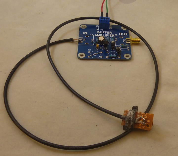
| + | * Cable using 18" RG-174 coax to input of RF Amp card | ||
| + | |||
| + | [[FILE:MicAmp_P952-720px.jpg]] | ||
| + | |||
| + | === Schematic Mods === | ||
| + | |||
| + | [[FILE:RF_Amp_Schematic-MODS.png]] | ||
| − | + | === Part Value Changes === | |
| − | |||
| − | |||
| − | |||
| − | + | * No transformers | |
| + | ** Transformers replaced by passives/jumpers | ||
| + | * R1 - 15K Ω | ||
| + | * R2 - 3K (small difference vs 3.3K on RF Amp) | ||
| + | * R3 - 120 Ω | ||
| + | * R4 - 10 Ω | ||
| + | * R5 - 50 Ω | ||
| + | ** Install R5 to simulate balanced modulator 50 Ω load | ||
| + | ** Install R5 on long leads to easily remove | ||
| + | * 33K Ω pullup to bias Electret mic | ||
| + | * T1 primary winding - 560 Ω | ||
| + | * C1 - 0.1 uF | ||
| + | * C2 - 10 uF | ||
| + | * C3 - 47 uF | ||
| + | * Add 10 uF capacitor from Vc point (transistor collector and 560 Ω resistor) to T1 output side | ||
| + | * Install output SMA connector | ||
| + | * Built SMA to RCA cable | ||
| + | ** Cut in half SMA male-male | ||
| + | ** Made 2 SMA to RCA cables | ||
| − | + | [[FILE:RF-Amp_MICAMP.PNG]] | |
| − | + | === Tested === | |
| − | |||
| − | |||
| − | |||
| − | |||
| − | |||
| − | |||
| − | |||
| − | [[ | + | * In application output goes to Balanced Modulator |
| + | ** Output level should be +7dBm for ADE-1 Mixers | ||
| + | * Tested into [[AudioAmp386]] - works | ||
| − | + | === Mic Amp LTspice Simulation === | |
| − | |||
| − | |||
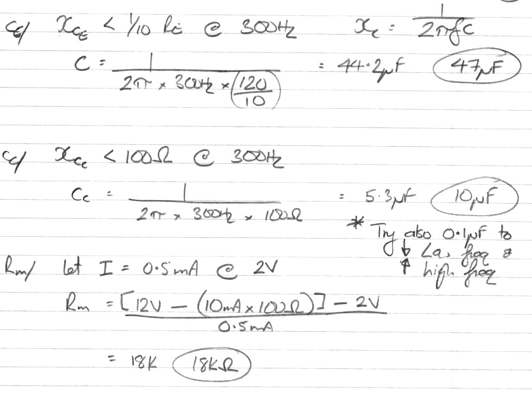
| − | + | * Low frequency response can be improved by increasing the value of the emitter bypass capacitor | |
| − | + | [[FILE:Mic_Amp_LTSpice_Sim.PNG]] | |
| − | * | + | * With 100uF cap across emitter resistor |
| − | |||
| − | |||
| − | |||
| − | [[ | + | [[FILE:Mic_Amp_Ce-100uF_LTSpice_Sim.PNG]] |
== Video == | == Video == | ||
Latest revision as of 22:30, 15 November 2021
Contents
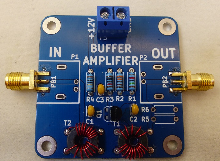
RF Amplifier Features
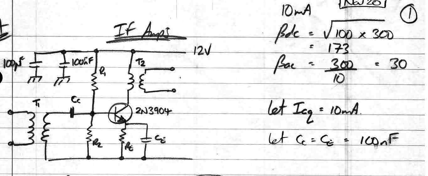
- Class A (Common Emitter) Amplifier
- Emitter resistor bypassed with capacitor for higher AC gain
- Transformer coupled input/output for impedance matching to 50Ω
- Capacitively coupled input
- Single 2N3904 NPN transistor
- Useful as an gain block in various applications
- Radio Transmitter/Receiver IF Amplifier
- Radio Transmitter/Receiver Antenna Amplifier
- Radio Transmitter Microphone amplifier (with minor modifications)
- As RF Amplifier
- Measured Gain Bandwidth (GBW) of 150
- Measured Gain @7 MHz, +25.2 dB at 12V
- Measured Gain @9 MHz, +24.7 dB at 12V
- Measured Gain @30 MHz, +13.8 dB at 12V
- As a microphone amplifier
- Approximately 20 dB at 1 KHz
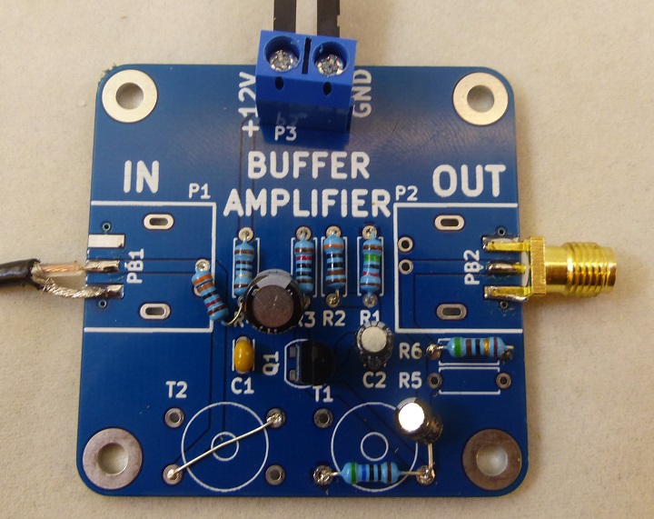
- Input connectors: SMA, BNC, or direct solder coax to SMA etches
- +12V nominal power
- 12-14 VDC
- 5 mm terminal block for power
- 49x49mm card
- 4x 4-40 mounting holes
Source Materials
- From Charlie Morris' (ZL2CTM) Go QRP Portable SSB Rig
- Charlie references Solid State Design for the Radio Amateur (pp 19-20)
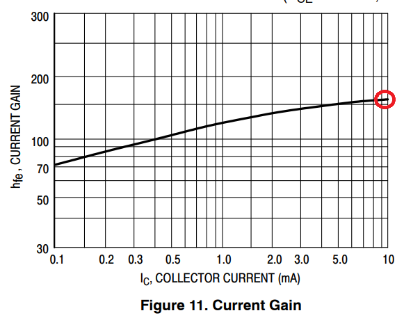
HFE at 10 mA
RF Amplifier Design
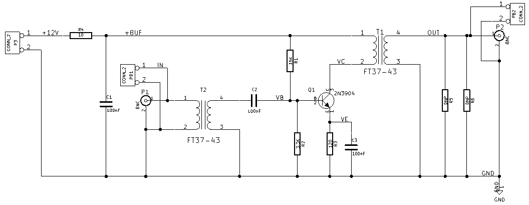
Schematic
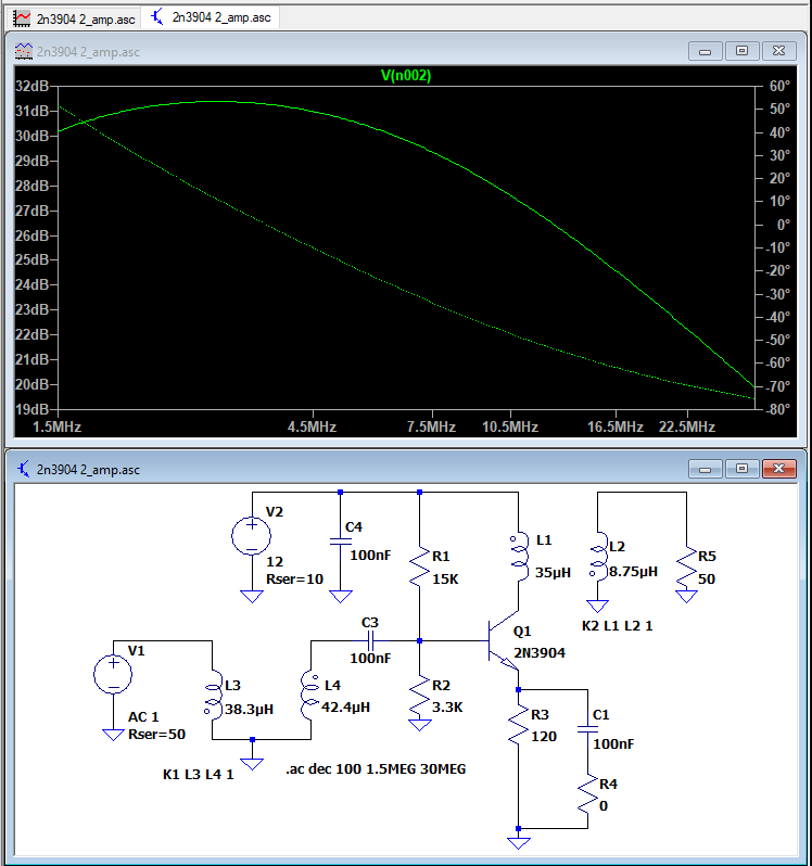
LT Spice Simulation
As Built - Rev 1
- LTspice Simulation - GitHub source file
- +28.4 dB at 9 MHz
Additional Resistor
- Insert 4.7 Ω resistor to emitter bypass capacitor
- Reduces maximum gain
- Increases gain over 1-30 MHz bandwidth
- Possible better for Antenna Amplifier application at lower frequencies
- +22.4 dB at 9 MHz
Charlie Morris Design Calculations
- From Charlie's notes with mods for my use
- Charlie Morris' (ZL2CTM) Go QRP Portable SSB Rig
- Charlie describes the design in detail in his video Simple SSB Rig: Part 6 - IF Amplifiers (Feb 2021)
- Based on the Class A RF Amplifier in Solid State Design for the Radio Amateur pp 19-20
- 2N3904 data sheet
- Emitter Resistance - helpful paper
Beta DC
- Geometric mean min/max beta at operating current
- =sqrt(100*300) = 173
Beta AC
- Gain bandwidth product divided by operating frequency
- Assume operating frequency of 9 MHz (IF frequency)
- = 300/9 = 33.3
DC Operating Point
- Max HFE RF gain at CE current of 10 mA
- If Vce = 6V, this is 60 mW power dissipation
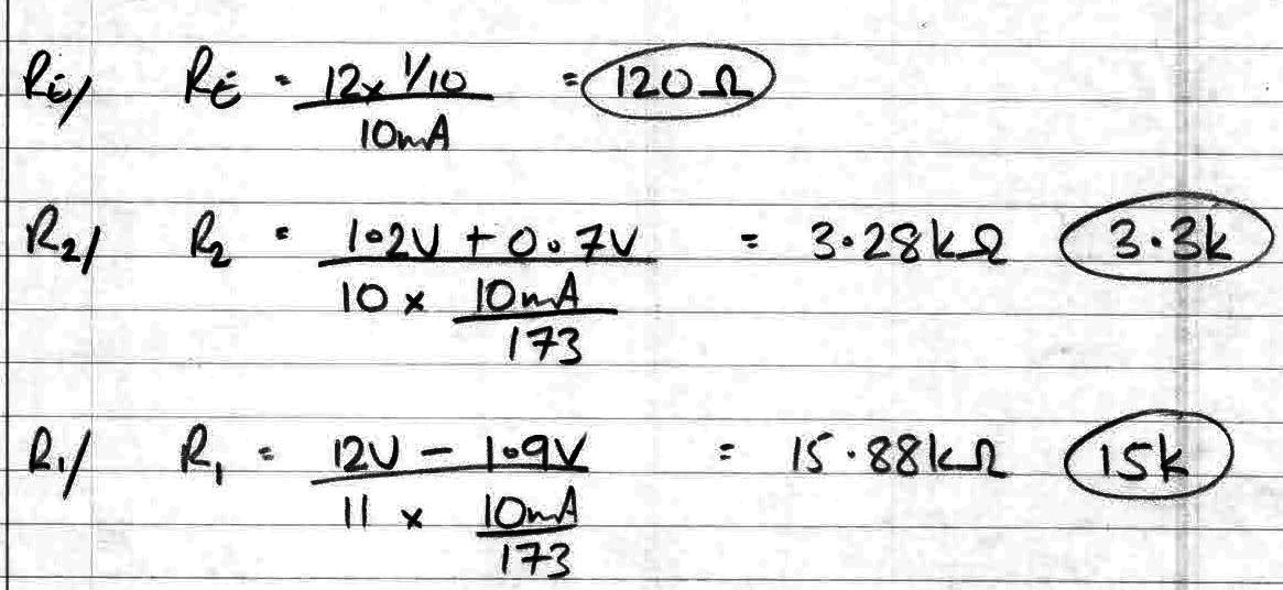
- Assume Ve (voltage across emitter resistor) = 1/10 Vcc = 12V/10 = 1.2V
- R3 is Re (emitter resistor) = 1.2V/0.01A = 120 Ω
- VCE = 0.7V (typical from data sheet)
- V(emitter) at 10% of Vcc rule of thumb = 1.2V
- V(base) = V(emitter) + VCE = 1.9V
- Base current is collector current divided by Beta DC
- Biasing resistors = 10x current needed by base current
- 10 mA in C-E, beta DC less = 10 mA/173 = 58 uA
- 10x the current in the biasing resistors = 580 uA (calculated)
- R2 is 1.9V at 580 uA = 3.29KΩ use 3.3KΩ
- R1 sources current to R2 and transistor base
- Voltage = Vcc (12V) - 1.9V = 10.1V
- Current = 577 uA + 58 uA = 635 uA
- R1 = 10.1 / .635 mA = 15.9KΩ, use 15KΩ
Measured DC operating point
- Measured with no input
- Vcc = 11.96V
- Current draw = 12 mA
- Quick test for wiring and more or less correct parts
- Expected 11 mA - close enough
- +BUFF = 11.84V
- 0.12V which is 12 mA through R4 at 10 Ω - expected
- V emitter = 1.41V
- 1.41V/12Ω = 11.75 mA close to 12 mA total measured current
- V on input divider = 2.06V
- Vbase + 0.7V - close
- Measured Vbe = 2.06-1.41 = 0.65 - close
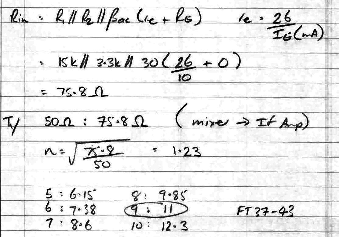
Input resistance
- Xc for 0.1uF cap from emitter to ground
- C=0.1uF
- F=10MHz
- 1/2*pi*F*C = 0.16Ω
- Parallel resistors R1, R2 paralleled with transistor input impedance
- R1=15KΩ, R2=3.3KΩ
- Transistor resistance = Beta AC (33.3) times re
- re = 26 / Ie (10 mA in mA) = 26/10 = 2.6
- SSDRA uses 25 as constant - close enough
- 26 comes from Ebers-Moll approximation
- Beta AC * re = 33.3*2.6 = 83.3Ω - predominates
- All in parallel are 80.8Ω
Gain calculation
- Approximation
- Ic = 0.01A
- Rc = 200
- Vrc = 2V
- Gain = Vrc / vt
- vt = 26 mV at room temperature
- Gain = 2V / .026V = 79.2 V/V
- Gain = +37 dB
Input/Output Transformers
- Using FT37-43 Toroid
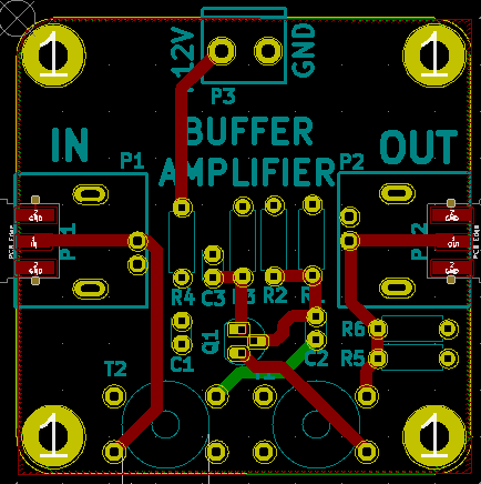
Tracks
Input Transformer
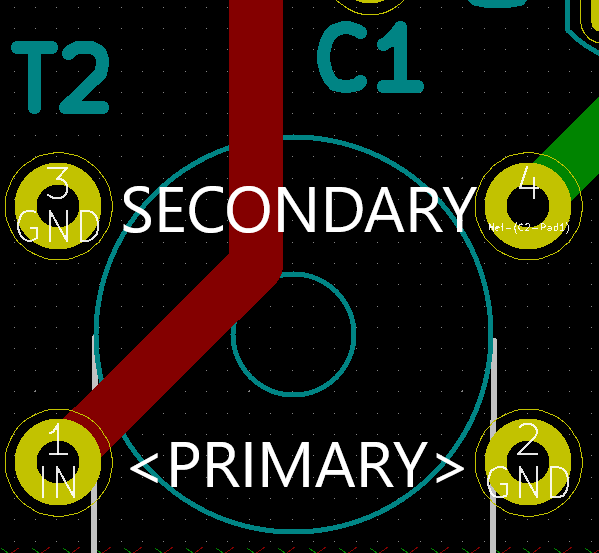
- Input Transformer (T1 on Charlie's - T2 on this board)
- Need to calculate turns ratio
- 50:80.8 Ω
- n = sqrt(Zout/Zin)sqrt(80.8/50) = 1.27 turns ratio
- Turns choices
- Minimum number of turns
- Rule of thumb - want Xl (coil impedance smallest value) to be least 4-5X the load
- Load = 80.8 Ω
- 5 * 80.8 Ω = 404.2 Ω minimum
- More turns = larger capacitance and drops bandwidth
- Toroid is FT37-43
- From Toroid page
- Xl = 404.4Ω at 9 MHz is 4.5 turns, round up to 5
- Try nearest integer numbers turns ratios
- 5:6 = 6% error
- 6:8 = -4.6%
- 7:9 = -1.1% << good choice
- 8:10 = +1.7%
- 9:11 = +4.0%
- 10:13 = -2.19%
- Use 7:9 turns ratio for optimal input transformer
Output Transformer
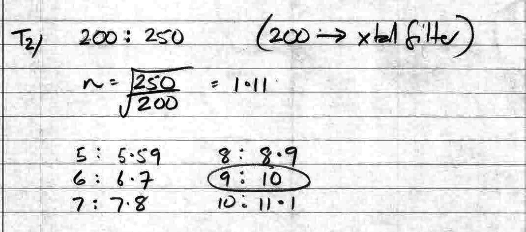
- Output transformer (T2 on Charlie's - T1 on this board)
- T2 - different than Charlie's design since my Crystal filters are all 50 Ω in/out
- SSDRA suggest presenting 200 Ω load to the collector
- Can't find reference in SSDRA
- Reflecting back 50 Ω load to 200 Ω collector...
- 200:50 Ω
- n = sqrt(200/50) = 2.0:1 turns ratio
- 10:5 turns
- 10 turns primary (on transistor collector)
- 10 turns = 35 uH
- 5 turns secondary (towards output)
- 5 turns = 8.75 uH
- 15 turns = 9.5 in
- 10 turns primary (on transistor collector)
Charlie's Notes
NanoVNA Measurements
- Goal: Measure RF-Amp performance using a NanoVNA running NanoSaver software on PC
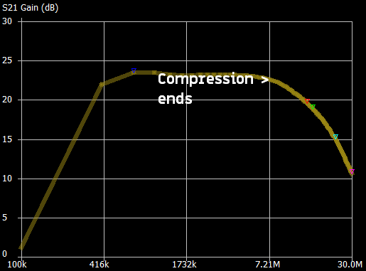
- S21 (gain) needs to be measured with a 40 dB attenuator on input to RF-Amp to avoid compression on the output
- S11 (reflection) input impedance can't be measured with input 40 dB attenuator because S11 just ends up measuring the attenuator
- Output should be terminated to 50 Ω for S11 measurement
- DC current = 12 mA
Measure S21
- Put 40 dB attenuator on RF-Amp input, measure S21 at output
- NanoVNA provides 50 Ω load to RF-Amp to properly terminate output
- Measure S21 with 9:11 input transformer
- S21 @ 100 KHz = -8 dB dB
- S21 @ 1.45 MHz = 35.4 dB (peak gain)
- S21 @ 9.1 MHz = 24.3 dB
- S21 @ 16 MHz = 20.1 dB
- S21 @ 30 MHz = 12.7 dB
- Peak gain justifies use of 40 dB attenuator to protect NanoVNA
LTspice vs NanoVNA
- LTspice simulation was pretty similar to NanoVNA results
- -10 dB at 100 KHz
- +32 dB at peak
- Lower output at higher frequencies
Measure Input Compression
- Is there compression if the NanoVNA drives the input directly?
- Test by driving directly from NanoVNA set to CW = 9 MHz
- Measured output with scope - not clipped at 9 MHz
- Approx. 1Vpp input = +22.1 dBm gain which matches the S21 with the attenuator on the input
- Vpp = 12.4V with 50 Ω load resistor
- Starts clipping at 7 Mhz and down
- Therefore, can measure input impedance at 9 MHz
- Other evidence of compression
- Compare S21 gain with no input attenuator, put external 40 dB RF Attenuators on output of RF-Amp to protect NanoVNA input
- S21 shows lower gain in lower frequencies so clipping/compression is happening
- Was: 35 dB at 1.4 MHz
- Is: 23.1 dB at 1.5 MHz
- Due to compression can't accurately measure lower frequencies with attenuator at output
- Compression below 7 MHz matches what was on scope
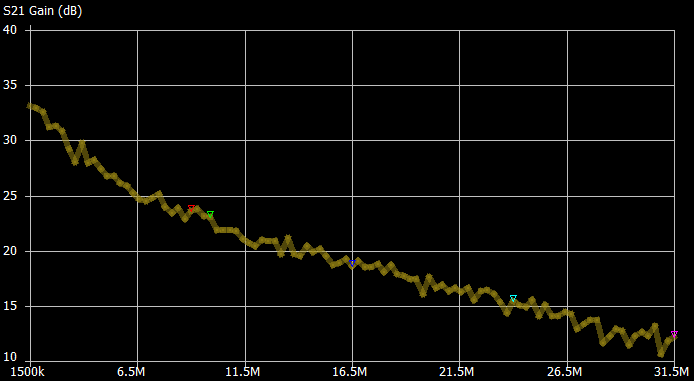
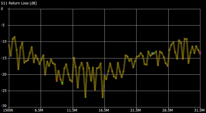
W2AEW S11 Measurement Method
- Can't drive the RF Amp directly from the NanoVNA
- High output level from the NanoVNA overdrives the RF Amp
- W2AEW provides a way of driving the RF Amp card without overdriving and still measure S11
- Calibrate NanoVNA using External 30 dB Attenuator
- See W2AEW #337 video above
- Insert 30 dB attenuator and calibrate with attenuator installed
- Open/sort/thru at the output side of the attenuator using NanoVNA RF Demo Kit
- NanoVNA RF Demo Kit has similar connectors, etc to RF Amp
- Scan 1-30 Mhz
- Overdriven at 1 MHz which "swamps" the RF Amp
- Re-calibrated at 1.5-31.5 MHz
- Peak gain at 1 MHz = 32 dB
- Does not overdrive the Amp or NanoVNA
- Downsize is a lot of noise in the return loss
- Peak gain at 1 MHz = 32 dB
- Tested two units
- Unit 1 has a 7:10 input transformer (T2) ratio
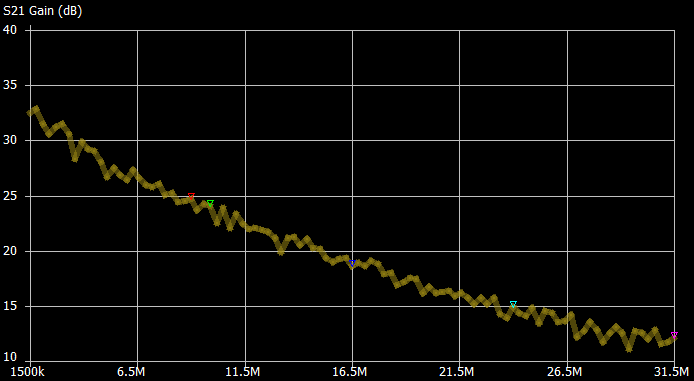
- Unit 2 has a 7:9 input transformer (T2) ratio
Unit 1
- 9 MHz measurements
- VSWR = 1.172
- S11 (Return Loss) = -22.014 dB
- S21 (Gain) = +23.624 dB
Unit 2
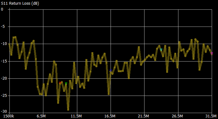
- 9 MHz measurement
- VSWR = 1.182
- S11 (Return Loss) = -21.565 dB
- S21 (Gain) = +24.656 dB
- 20 dB gain at 15 MHz
- Gain Bandwidth (GBW) = ~150
- GBW is a good predictor of gain at particular frequencies
- Calculated Gain of 14 dB at 30 MHz - measured at +12.8 dB
- Measured at +26 dB at 7 MHz
Compare RF Amp vs Kits and Parts Amp
- RF-Amp
- 2N3904 transistor
- Ft is is 300
- Measured at 150 GBW
- Kits and Parts - Universal Wideband Small Signal RF Amplifier
- 2SC5551A transistor
- Much higher Ft 3.5 GHz
- Gain is much flatter over bandwidth
- 1.5 Mhz = 26.6 dB
- 30 Mhz = 24.9 dB
- Gain is much flatter over bandwidth
- Good as broadband amplifier
- Both would be equivalent at 9 MHz as IF Amp
- Kits and Parts would be better as Antenna Amplifier
- RF Amp card current draws 11 mA
- Kits and Parts card current draws 30 mA
Use of Card as a Microphone Amp
- Charlie's video
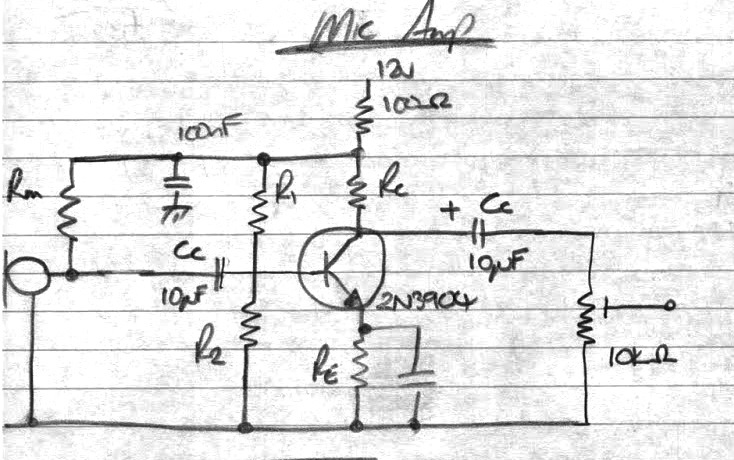
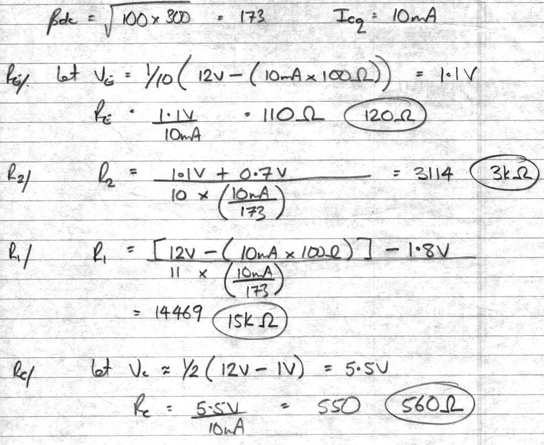
Charlie's Schematic/Calculations
- Charlie's page
- This was from a couple of months later than the video
Test with Electret Microphone
- Charlie assumes voltage/current - didn't measure
- I chose to determine Electret operating point through measurement
- DC powered
- AC coupled output
- 13.8VDC (max) power
- Attach decade resistor box between power supply + side and Electret mic + side
- Adjust decade resistance value to measure 4V across mic with 13.8 VDC supply
- 2V with 12V power supply
- Selected value = 33K Ω pullup to 13.8V gets 4V across mic
- 2V out with 12V supply
- Secure with zip ties and secure with superglue
Wiring up Mic to Amp
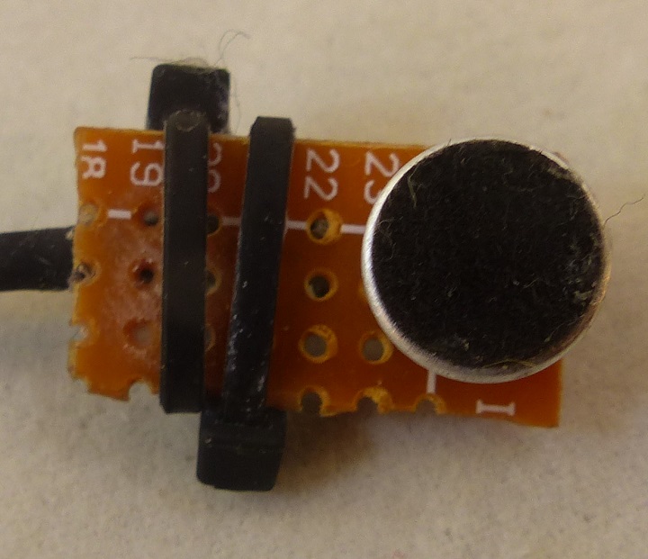
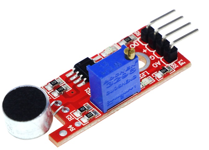
- Electret Condenser Microphone
- Removed from KY-037 microphone (Arduino sensor card)
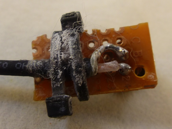
- Install Electret Condenser Microphone on small perf board
- Cable using 18" RG-174 coax to input of RF Amp card
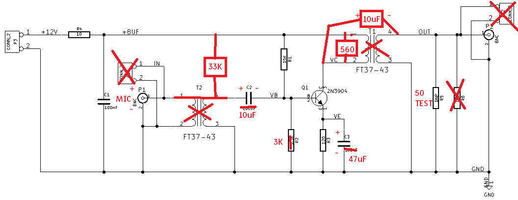
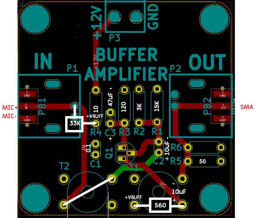
Schematic Mods
Part Value Changes
- No transformers
- Transformers replaced by passives/jumpers
- R1 - 15K Ω
- R2 - 3K (small difference vs 3.3K on RF Amp)
- R3 - 120 Ω
- R4 - 10 Ω
- R5 - 50 Ω
- Install R5 to simulate balanced modulator 50 Ω load
- Install R5 on long leads to easily remove
- 33K Ω pullup to bias Electret mic
- T1 primary winding - 560 Ω
- C1 - 0.1 uF
- C2 - 10 uF
- C3 - 47 uF
- Add 10 uF capacitor from Vc point (transistor collector and 560 Ω resistor) to T1 output side
- Install output SMA connector
- Built SMA to RCA cable
- Cut in half SMA male-male
- Made 2 SMA to RCA cables
Tested
- In application output goes to Balanced Modulator
- Output level should be +7dBm for ADE-1 Mixers
- Tested into AudioAmp386 - works
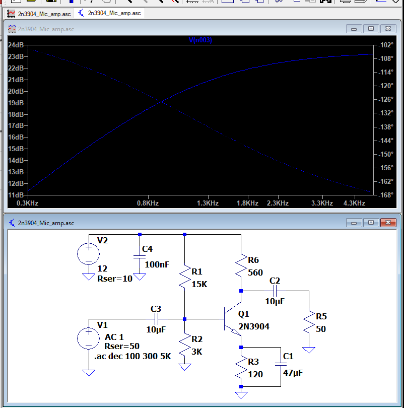
Mic Amp LTspice Simulation
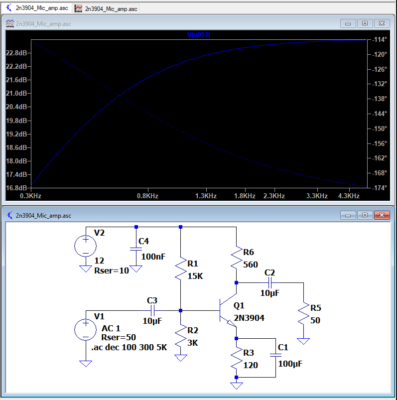
- Low frequency response can be improved by increasing the value of the emitter bypass capacitor
- With 100uF cap across emitter resistor
Video
