Difference between revisions of "QM Tech Cyclone V FPGA Board"
Jump to navigation
Jump to search
Blwikiadmin (talk | contribs) |
Blwikiadmin (talk | contribs) |
||
| (One intermediate revision by the same user not shown) | |||
| Line 3: | Line 3: | ||
== Features == | == Features == | ||
| + | * Mounts to [[RETRO-EP4CE15]] | ||
* [https://www.aliexpress.com/item/1000006622149.html?spm=a2g0s.9042311.0.0.3e1f4c4dZLO3HX QMTECH Altera Intel FPGA Core Board Cyclone V CycloneV 5CEFA2F23 SDRAM] | * [https://www.aliexpress.com/item/1000006622149.html?spm=a2g0s.9042311.0.0.3e1f4c4dZLO3HX QMTECH Altera Intel FPGA Core Board Cyclone V CycloneV 5CEFA2F23 SDRAM] | ||
** [https://github.com/ChinaQMTECH/CYCLONE_IV_EP4CE15 QMTECH GitHub page] | ** [https://github.com/ChinaQMTECH/CYCLONE_IV_EP4CE15 QMTECH GitHub page] | ||
| Line 85: | Line 86: | ||
== Programming the FPGA EEPROM == | == Programming the FPGA EEPROM == | ||
| − | |||
| − | |||
| − | |||
| − | |||
* EEPROM marked as 8HA15 | * EEPROM marked as 8HA15 | ||
| Line 94: | Line 91: | ||
* Convert Programming File | * Convert Programming File | ||
* Configuration Device = MT25QL128 | * Configuration Device = MT25QL128 | ||
| − | |||
| − | |||
| − | |||
| − | |||
| − | |||
| − | |||
| − | |||
| − | |||
| − | |||
| − | |||
| − | |||
| − | |||
| − | |||
| − | |||
| − | |||
| − | |||
| − | |||
| − | |||
| − | |||
| − | |||
* Mode = Active Serial | * Mode = Active Serial | ||
* Programming File Type: *.jic | * Programming File Type: *.jic | ||
Latest revision as of 00:10, 22 May 2022
Contents
Features
- Mounts to RETRO-EP4CE15
- QMTECH Altera Intel FPGA Core Board Cyclone V CycloneV 5CEFA2F23 SDRAM
- QMTECH GitHub page
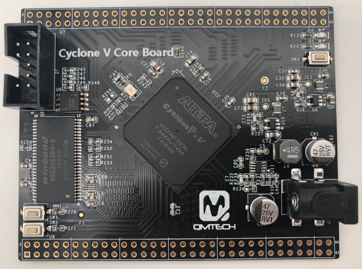
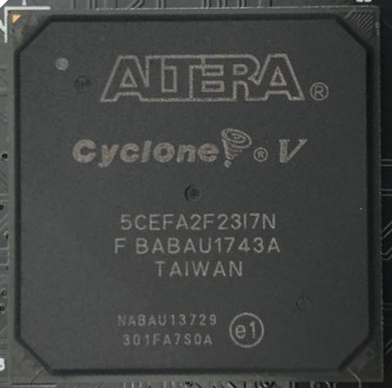
- On-Board FPGA: 5CEFA2F23I7N
- On-Board FPGA external crystal frequency: 50MHz
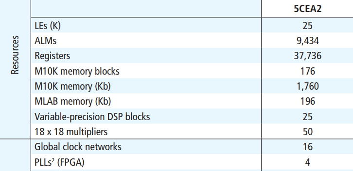
- 5CEFA2F23 has rich RAM resource up to 1,760Kb
- 5CEFA2F23 has 25K logic cells
- On-Board Micron MT25QL128A SPI Flash, 16M bytes for user configuration code
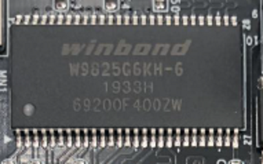
- On-Board Winbond 32MB SDRAM, W9825G6KH-6
- On-Board 3.3V power supply for FPGA by using MP2315 wide input range DC/DC
- 5CEFA2F23 core board has two 64p, 2.54mm pitch headers for extending 108 user IOs. All 108 user IOs are precisely designed with length matching
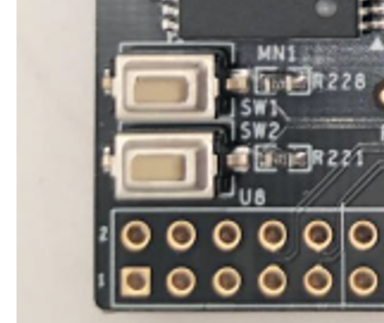
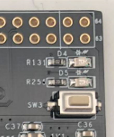
- 5CEFA2F23 core board has 3 user switches
- 5CEFA2F23 core board has 2 user LEDs
- 5CEFA2F23 core board has JTAG interface, by using 10p, 2.54mm pitch header
- 5CEFA2F23 core board PCB size is: 6.7cm x 8.4cm
- Default power source for board is: 1A@5V DC, the DC header type: DC-050, 5.5mmx2.1mm
FPGA
5CEFA2F23 FPGA Resources
- CLK_50M = PIN_M9
LEDs/Switches
- Power LED = D4 (On when 5V is applied)
- User LED = LED_D5 = FPGA PIN_D17
- KEY0 = SW1 = FPGA PIN_AB13
- RESET_N = SW2 = FPGA PIN_V18
- nCONFIG = SW3 = FPGA PIN_A4
- JP5 - 5V
SDRAM
SDRAM Pins
- sdRamClk = PIN_AB11
- sdRamClkEn = PIN_V9
- n_sdRamCas = PIN_AA7
- n_sdRamCe = PIN_AB5
- n_sdRamRas = PIN_AB6
- n_sdRamWe = PIN_W9
- sdRamAddr[0] = PIN_P8
- sdRamAddr[1] = PIN_P7
- sdRamAddr[2] = PIN_N8
- sdRamAddr[3] = PIN_N6
- sdRamAddr[4] = PIN_U6
- sdRamAddr[5] = PIN_U7
- sdRamAddr[6] = PIN_V6
- sdRamAddr[7] = PIN_U8
- sdRamAddr[8] = PIN_T8
- sdRamAddr[9] = PIN_W8
- sdRamAddr[10] = PIN_R6
- sdRamAddr[11] = PIN_T9
- sdRamAddr[12] = PIN_Y9
- sdRamAddr[13] = PIN_T7
- sdRamAddr[14] = PIN_P9
- sdRamData[0] = PIN_AA12
- sdRamData[1] = PIN_Y11
- sdRamData[2] = PIN_AA10
- sdRamData[3] = PIN_AB10
- sdRamData[4] = PIN_Y10
- sdRamData[5] = PIN_AA9
- sdRamData[6] = PIN_AB8
- sdRamData[7] = PIN_AA8
- sdRamData[8] = PIN_U10
- sdRamData[9] = PIN_T10
- sdRamData[10] = PIN_U11
- sdRamData[11] = PIN_R10
- sdRamData[12] = PIN_R11
- sdRamData[13] = PIN_U12
- sdRamData[14] = PIN_R12
- sdRamData[15] = PIN_P12
Programming the FPGA EEPROM
- EEPROM marked as 8HA15
- File
- Convert Programming File
- Configuration Device = MT25QL128
- Mode = Active Serial
- Programming File Type: *.jic
- Advanced = Check both Disables...
- Select Flash Loader
- Add Device = Cyclone V and 5CEFA2
- Select SOF Data
- Select Add File and select the .sof file
- Generate
- In Tools, Programmer
- Mode: JTAG
- Add file and select the .jic file
- Select Program/Configure
- Takes a while to program
- Press button near VGA
Pin List (5CEFA2F23I7 on RETRO-EP4CE15)
set_global_assignment -name FAMILY "Cyclone V" set_global_assignment -name DEVICE 5CEFA2F23I7 set_global_assignment -name TOP_LEVEL_ENTITY TS2_68000_Top set_global_assignment -name ORIGINAL_QUARTUS_VERSION 18.1.0 set_global_assignment -name PROJECT_CREATION_TIME_DATE "07:21:26 JULY 04, 2020" set_global_assignment -name LAST_QUARTUS_VERSION "18.1.0 Lite Edition" set_global_assignment -name PROJECT_OUTPUT_DIRECTORY output_files set_global_assignment -name MIN_CORE_JUNCTION_TEMP "-40" set_global_assignment -name MAX_CORE_JUNCTION_TEMP 100 set_global_assignment -name ERROR_CHECK_FREQUENCY_DIVISOR 1 set_global_assignment -name EDA_SIMULATION_TOOL "ModelSim-Altera (VHDL)" set_global_assignment -name EDA_TIME_SCALE "1 ps" -section_id eda_simulation set_global_assignment -name EDA_OUTPUT_DATA_FORMAT VHDL -section_id eda_simulation set_global_assignment -name PARTITION_NETLIST_TYPE SOURCE -section_id Top set_global_assignment -name PARTITION_FITTER_PRESERVATION_LEVEL PLACEMENT_AND_ROUTING -section_id Top set_global_assignment -name PARTITION_COLOR 16764057 -section_id Top set_global_assignment -name POWER_PRESET_COOLING_SOLUTION "23 MM HEAT SINK WITH 200 LFPM AIRFLOW" set_global_assignment -name POWER_BOARD_THERMAL_MODEL "NONE (CONSERVATIVE)" set_global_assignment -name TIMING_ANALYZER_MULTICORNER_ANALYSIS ON set_global_assignment -name SMART_RECOMPILE ON set_global_assignment -name STRATIX_DEVICE_IO_STANDARD "3.3-V LVTTL" # Clock and reset set_location_assignment PIN_M9 -to i_CLOCK_50 set_location_assignment PIN_V18 -to n_reset set_instance_assignment -name WEAK_PULL_UP_RESISTOR ON -to n_reset # Serial set_location_assignment PIN_B11 -to cts1 set_location_assignment PIN_F10 -to rts1 set_location_assignment PIN_C11 -to rxd1 set_location_assignment PIN_G10 -to txd1 set_instance_assignment -name WEAK_PULL_UP_RESISTOR ON -to rxd1 set_location_assignment PIN_L17 -to serSelect set_instance_assignment -name WEAK_PULL_UP_RESISTOR ON -to serSelect # SRAM set_location_assignment PIN_E2 -to n_sRamCS set_location_assignment PIN_L2 -to n_sRamOE set_location_assignment PIN_D6 -to n_sRamWE set_location_assignment PIN_E9 -to sramAddress[19] set_location_assignment PIN_B5 -to sramAddress[18] set_location_assignment PIN_B6 -to sramAddress[17] set_location_assignment PIN_A7 -to sramAddress[16] set_location_assignment PIN_A10 -to sramAddress[15] set_location_assignment PIN_A9 -to sramAddress[14] set_location_assignment PIN_B7 -to sramAddress[13] set_location_assignment PIN_A5 -to sramAddress[12] set_location_assignment PIN_D9 -to sramAddress[11] set_location_assignment PIN_C6 -to sramAddress[10] set_location_assignment PIN_E7 -to sramAddress[9] set_location_assignment PIN_G2 -to sramAddress[8] set_location_assignment PIN_N2 -to sramAddress[7] set_location_assignment PIN_U2 -to sramAddress[6] set_location_assignment PIN_W2 -to sramAddress[5] set_location_assignment PIN_Y3 -to sramAddress[4] set_location_assignment PIN_U1 -to sramAddress[3] set_location_assignment PIN_N1 -to sramAddress[2] set_location_assignment PIN_L1 -to sramAddress[1] set_location_assignment PIN_G1 -to sramAddress[0] set_location_assignment PIN_C1 -to sramData[0] set_location_assignment PIN_G6 -to sramData[1] set_location_assignment PIN_G8 -to sramData[2] set_location_assignment PIN_F7 -to sramData[3] set_location_assignment PIN_H8 -to sramData[4] set_location_assignment PIN_H6 -to sramData[5] set_location_assignment PIN_C2 -to sramData[6] set_location_assignment PIN_D3 -to sramData[7] # SD Card set_location_assignment PIN_B15 -to sdCS set_location_assignment PIN_B16 -to sdMISO set_location_assignment PIN_C15 -to sdMOSI set_location_assignment PIN_C16 -to sdSCLK set_location_assignment PIN_D17 -to driveLED set_instance_assignment -name WEAK_PULL_UP_RESISTOR ON -to sdMISO # Video set_location_assignment PIN_A15 -to hSync set_location_assignment PIN_D12 -to videoR1 set_location_assignment PIN_E12 -to videoR0 set_location_assignment PIN_C13 -to videoG1 set_location_assignment PIN_D13 -to videoG0 set_location_assignment PIN_A13 -to videoB1 set_location_assignment PIN_B13 -to videoB0 set_location_assignment PIN_A14 -to vSync # PS/2 set_location_assignment PIN_AA2 -to ps2Clk set_location_assignment PIN_AA1 -to ps2Data set_instance_assignment -name WEAK_PULL_UP_RESISTOR ON -to ps2Clk set_instance_assignment -name WEAK_PULL_UP_RESISTOR ON -to ps2Data # SDRAM set_location_assignment PIN_AB11 -to sdRamClk set_location_assignment PIN_V9 -to sdRamClkEn set_location_assignment PIN_AA7 -to n_sdRamCas set_location_assignment PIN_AB5 -to n_sdRamCe set_location_assignment PIN_AB6 -to n_sdRamRas set_location_assignment PIN_W9 -to n_sdRamWe set_location_assignment PIN_AB7 -to DQML set_location_assignment PIN_V10 -to DQMH set_location_assignment PIN_P9 -to sdRamBA[1] set_location_assignment PIN_T7 -to sdRamBA[0] set_location_assignment PIN_Y9 -to sdRamAddr[12] set_location_assignment PIN_T9 -to sdRamAddr[11] set_location_assignment PIN_R6 -to sdRamAddr[10] set_location_assignment PIN_W8 -to sdRamAddr[9] set_location_assignment PIN_T8 -to sdRamAddr[8] set_location_assignment PIN_U8 -to sdRamAddr[7] set_location_assignment PIN_V6 -to sdRamAddr[6] set_location_assignment PIN_U7 -to sdRamAddr[5] set_location_assignment PIN_U6 -to sdRamAddr[4] set_location_assignment PIN_N6 -to sdRamAddr[3] set_location_assignment PIN_N8 -to sdRamAddr[2] set_location_assignment PIN_P7 -to sdRamAddr[1] set_location_assignment PIN_P8 -to sdRamAddr[0] set_location_assignment PIN_P12 -to sdRamData[15] set_location_assignment PIN_R12 -to sdRamData[14] set_location_assignment PIN_U12 -to sdRamData[13] set_location_assignment PIN_R11 -to sdRamData[12] set_location_assignment PIN_R10 -to sdRamData[11] set_location_assignment PIN_U11 -to sdRamData[10] set_location_assignment PIN_T10 -to sdRamData[9] set_location_assignment PIN_U10 -to sdRamData[8] set_location_assignment PIN_AA8 -to sdRamData[7] set_location_assignment PIN_AB8 -to sdRamData[6] set_location_assignment PIN_AA9 -to sdRamData[5] set_location_assignment PIN_Y10 -to sdRamData[4] set_location_assignment PIN_AB10 -to sdRamData[3] set_location_assignment PIN_AA10 -to sdRamData[2] set_location_assignment PIN_Y11 -to sdRamData[1] set_location_assignment PIN_AA12 -to sdRamData[0] #50-pin I/O Connector set_location_assignment PIN_AB15 -to IO_PIN[3] set_location_assignment PIN_AA15 -to IO_PIN[4] set_location_assignment PIN_Y14 -to IO_PIN[5] set_location_assignment PIN_Y15 -to IO_PIN[6] set_location_assignment PIN_AB17 -to IO_PIN[7] set_location_assignment PIN_AB18 -to IO_PIN[8] set_location_assignment PIN_Y16 -to IO_PIN[9] set_location_assignment PIN_Y17 -to IO_PIN[10] set_location_assignment PIN_AA17 -to IO_PIN[11] set_location_assignment PIN_AA18 -to IO_PIN[12] set_location_assignment PIN_AA19 -to IO_PIN[13] set_location_assignment PIN_AA20 -to IO_PIN[14] set_location_assignment PIN_Y19 -to IO_PIN[15] set_location_assignment PIN_Y20 -to IO_PIN[16] set_location_assignment PIN_AB20 -to IO_PIN[17] set_location_assignment PIN_AB21 -to IO_PIN[18] set_location_assignment PIN_AB22 -to IO_PIN[19] set_location_assignment PIN_AA22 -to IO_PIN[20] set_location_assignment PIN_Y22 -to IO_PIN[21] set_location_assignment PIN_W22 -to IO_PIN[22] set_location_assignment PIN_W21 -to IO_PIN[23] set_location_assignment PIN_Y21 -to IO_PIN[24] set_location_assignment PIN_V21 -to IO_PIN[25] set_location_assignment PIN_U22 -to IO_PIN[26] set_location_assignment PIN_W19 -to IO_PIN[27] set_location_assignment PIN_V20 -to IO_PIN[28] set_location_assignment PIN_U20 -to IO_PIN[29] set_location_assignment PIN_U21 -to IO_PIN[30] set_location_assignment PIN_T22 -to IO_PIN[31] set_location_assignment PIN_R22 -to IO_PIN[32] set_location_assignment PIN_R21 -to IO_PIN[33] set_location_assignment PIN_P22 -to IO_PIN[34] set_location_assignment PIN_T19 -to IO_PIN[35] set_location_assignment PIN_T20 -to IO_PIN[36] set_location_assignment PIN_P17 -to IO_PIN[37] set_location_assignment PIN_P16 -to IO_PIN[38] set_location_assignment PIN_N21 -to IO_PIN[39] set_location_assignment PIN_N20 -to IO_PIN[40] set_location_assignment PIN_M20 -to IO_PIN[41] set_location_assignment PIN_M21 -to IO_PIN[42] set_location_assignment PIN_N19 -to IO_PIN[43] set_location_assignment PIN_M18 -to IO_PIN[44] set_location_assignment PIN_L19 -to IO_PIN[45] set_location_assignment PIN_L18 -to IO_PIN[46] set_location_assignment PIN_L22 -to IO_PIN[47] set_location_assignment PIN_M22 -to IO_PIN[48] # set_global_assignment -name ENABLE_SIGNALTAP OFF set_global_assignment -name USE_SIGNALTAP_FILE stp1.stp set_global_assignment -name ENABLE_OCT_DONE OFF set_global_assignment -name ENABLE_CONFIGURATION_PINS OFF set_global_assignment -name ENABLE_BOOT_SEL_PIN OFF set_global_assignment -name USE_CONFIGURATION_DEVICE OFF set_global_assignment -name CRC_ERROR_OPEN_DRAIN OFF set_global_assignment -name RESERVE_FLASH_NCE_AFTER_CONFIGURATION "USE AS REGULAR IO" set_global_assignment -name OUTPUT_IO_TIMING_NEAR_END_VMEAS "HALF VCCIO" -rise set_global_assignment -name OUTPUT_IO_TIMING_NEAR_END_VMEAS "HALF VCCIO" -fall set_global_assignment -name OUTPUT_IO_TIMING_FAR_END_VMEAS "HALF SIGNAL SWING" -rise set_global_assignment -name OUTPUT_IO_TIMING_FAR_END_VMEAS "HALF SIGNAL SWING" -fall set_global_assignment -name CYCLONEII_RESERVE_NCEO_AFTER_CONFIGURATION "USE AS REGULAR IO" set_global_assignment -name RESERVE_DATA1_AFTER_CONFIGURATION "USE AS REGULAR IO" set_global_assignment -name RESERVE_DATA0_AFTER_CONFIGURATION "USE AS REGULAR IO" set_global_assignment -name RESERVE_DCLK_AFTER_CONFIGURATION "USE AS REGULAR IO" set_global_assignment -name VHDL_FILE "../../MultiComp (VHDL Template)/Components/Debounce/LongDebounce/debounce.vhd" set_global_assignment -name VHDL_FILE Components/RAM_16Kx16.vhd set_global_assignment -name VHDL_FILE Components/RAM_4Kx16.vhd set_global_assignment -name VHDL_FILE "../../MultiComp (VHDL Template)/Components/TERMINAL/SBCTextDisplayRGB.vhd" set_global_assignment -name VHDL_FILE "../../MultiComp (VHDL Template)/Components/TERMINAL/SansBoldRomReduced.vhd" set_global_assignment -name VHDL_FILE "../../MultiComp (VHDL Template)/Components/TERMINAL/SansBoldRom.vhd" set_global_assignment -name VHDL_FILE "../../MultiComp (VHDL Template)/Components/TERMINAL/DisplayRam2K.vhd" set_global_assignment -name VHDL_FILE "../../MultiComp (VHDL Template)/Components/TERMINAL/DisplayRam1K.vhd" set_global_assignment -name VHDL_FILE "../../MultiComp (VHDL Template)/Components/TERMINAL/CGABoldRomReduced.vhd" set_global_assignment -name VHDL_FILE "../../MultiComp (VHDL Template)/Components/TERMINAL/CGABoldRom.vhd" set_global_assignment -name VHDL_FILE "../../MultiComp (VHDL Template)/Components/UART/bufferedUART.vhd" set_global_assignment -name VHDL_FILE "../../MultiComp (VHDL template)/Components/CPU/M68000/TG68K_2013/TG68KdotC_Kernel.vhd" set_global_assignment -name VHDL_FILE "../../MultiComp (VHDL Template)/Components/CPU/M68000/TG68K_2013/TG68K_Pack.vhd" set_global_assignment -name VHDL_FILE "../../MultiComp (VHDL Template)/Components/CPU/M68000/TG68K_2013/TG68K_ALU.vhd" set_global_assignment -name VHDL_FILE TS2_68000_Top.vhd set_global_assignment -name QIP_FILE Components/Monitor_68K_ROM.qip set_global_assignment -name QIP_FILE Components/RAM_8Kx16.qip set_global_assignment -name NUM_PARALLEL_PROCESSORS ALL set_instance_assignment -name PARTITION_HIERARCHY root_partition -to | -section_id Top >/pre>Resources
* GitHub Repo
