Difference between revisions of "TinyOptoProbe"
Blwikiadmin (talk | contribs) |
Blwikiadmin (talk | contribs) |
||
| Line 1: | Line 1: | ||
| − | TinyOptoProbe-CCA-X2-ExtCable-02-640.jpg | + | [[File:TinyOptoProbe-CCA-X2-ExtCable-02-640.jpg]] |
== What is a TinyOptoProbe == | == What is a TinyOptoProbe == | ||
| Line 11: | Line 11: | ||
I needed it to debug opto-isolator inputs. I couldn't get to the output that was driving the opto-isolator because it was an a conformal coated card. Add to that the far end was driving the opto-isolator low with an open collector driver. The other side of the source was connected to a resistor pulled up to 5V power. There was no place I could hook a scope since there was no externally accessible ground point. I could probably have attached an LED in place of the opto and watched the light go on and off but what if there was a short pulse which I could not see? I needed an old fashioned logic probe but with a major difference. The logic probe had to be completely isolated from the unit under test and old fashioned logic probes require attaching the the ground. So I came up with the TinyOptoProbe. | I needed it to debug opto-isolator inputs. I couldn't get to the output that was driving the opto-isolator because it was an a conformal coated card. Add to that the far end was driving the opto-isolator low with an open collector driver. The other side of the source was connected to a resistor pulled up to 5V power. There was no place I could hook a scope since there was no externally accessible ground point. I could probably have attached an LED in place of the opto and watched the light go on and off but what if there was a short pulse which I could not see? I needed an old fashioned logic probe but with a major difference. The logic probe had to be completely isolated from the unit under test and old fashioned logic probes require attaching the the ground. So I came up with the TinyOptoProbe. | ||
| − | TinyOptoProbe-input-test.PNG | + | [[File:TinyOptoProbe-input-test.PNG]] |
This board allows signals to be monitored in an isolated manner from the circuit being monitored. The downside is that it requires 10 mA from the circuit under test to operate. This board is used where measurement of an opto circuit doesn't allow ground clips to be connected to the device under test. | This board allows signals to be monitored in an isolated manner from the circuit being monitored. The downside is that it requires 10 mA from the circuit under test to operate. This board is used where measurement of an opto circuit doesn't allow ground clips to be connected to the device under test. | ||
| Line 17: | Line 17: | ||
== Features == | == Features == | ||
| − | Isolated Opto-coupled input | + | * Isolated Opto-coupled input |
| − | 10 mA nominal input current loop | + | ** 10 mA nominal input current loop |
| − | All current is returned on the test ground | + | ** All current is returned on the test ground |
| − | No current loop from the Unit Under Test to the logic on the card | + | ** No current loop from the Unit Under Test to the logic on the card |
| − | Isolation voltage dependent upon the opto-coupler selected but typically 500 V min | + | ** Isolation voltage dependent upon the opto-coupler selected but typically 500 V min |
| − | 5V, 12V, or 24V input levels | + | * 5V, 12V, or 24V input levels |
| − | Works with relay circuits for monitoring relay contacts | + | ** Works with relay circuits for monitoring relay contacts |
| − | Two LEDs (High/Low and Pulse) | + | * Two LEDs (High/Low and Pulse) |
| − | ATTiny85 microproceasor based | + | * ATTiny85 microproceasor based |
| − | Program to monitor the input and flash the Pulse LED if there is a change (H>L or L>H) | + | ** Program to monitor the input and flash the Pulse LED if there is a change (H>L or L>H) |
| − | DC power input | + | * DC power input |
| − | 9V power | + | ** 9V power |
| − | Can be run from a wall wart power supply or a 9V battery | + | *** Can be run from a wall wart power supply or a 9V battery |
| − | Low power consumption, 25 mA max | + | ** Low power consumption, 25 mA max |
| − | 25 mA when both LEDs are on | + | ** 25 mA when both LEDs are on |
| − | 10 mA when one LED is on | + | ** 10 mA when one LED is on |
| − | Small form factor 26x49mm | + | * Small form factor 26x49mm |
| − | (4) 4-40 mounting holes | + | * (4) 4-40 mounting holes |
== Operation - Test Opto-Coupler Connection == | == Operation - Test Opto-Coupler Connection == | ||
| Line 45: | Line 45: | ||
== Input Circuit == | == Input Circuit == | ||
| − | TinyOptoProbe-x1-input.PNG | + | [[File:TinyOptoProbe-x1-input.PNG]] |
== Layout == | == Layout == | ||
| − | TinyOptoProbe-X2-PWB-Layers-Kicad.png | + | [[File:TinyOptoProbe-X2-PWB-Layers-Kicad.png]] |
== Connectors/Headers == | == Connectors/Headers == | ||
| Line 55: | Line 55: | ||
=== H1 VREG power header (X1 board only) === | === H1 VREG power header (X1 board only) === | ||
| − | Install shunt to power card from the DC jack. | + | * Install shunt to power card from the DC jack. |
| − | Remove shunt to program Microprocessor from ISP connector (H2). | + | * Remove shunt to program Microprocessor from ISP connector (H2). |
=== H2 ISP Connector (X2 Board) === | === H2 ISP Connector (X2 Board) === | ||
| − | TinyOptoProbe-X2-PWB-H2-Header.png | + | [[File:TinyOptoProbe-X2-PWB-H2-Header.png]] |
This is a strange shaped 7-pin header. This header serves a dual purpose. | This is a strange shaped 7-pin header. This header serves a dual purpose. | ||
| − | Pin 2 is used for both the ICSP and power select jumpers. | + | * Pin 2 is used for both the ICSP and power select jumpers. |
| − | This effectively prevents the board from being powered by both the ICSP and voltage regulator at the same time. | + | ** This effectively prevents the board from being powered by both the ICSP and voltage regulator at the same time. |
| − | If a shunt is installed into pins 2 and 7 the power for the card will come from the voltage regulator on the card. | + | ** If a shunt is installed into pins 2 and 7 the power for the card will come from the voltage regulator on the card. |
| − | Pins 1-6 are the normal pinout for In-Circuit System Programmer (ICSP) pins. | + | * Pins 1-6 are the normal pinout for In-Circuit System Programmer (ICSP) pins. |
=== H2 ISP Connector (X1 Board) === | === H2 ISP Connector (X1 Board) === | ||
| − | TinyOptoProbe-x1-ISP.PNG | + | [[File:TinyOptoProbe-x1-ISP.PNG]] |
=== J1 - Power Connector === | === J1 - Power Connector === | ||
| − | GND - shell | + | # GND - shell |
| − | +7 to +9V - center pin | + | # +7 to +9V - center pin |
| − | P1 - Input Connector | + | |
| − | GND | + | === P1 - Input Connector === |
| − | +5V | + | |
| − | +12V | + | # GND |
| − | +24V | + | # +5V |
| + | # +12V | ||
| + | # +24V | ||
== Software == | == Software == | ||
| − | OptoProbe Code | + | * [https://github.com/douggilliland/lb-Arduino-Code/tree/master/OptoProbe OptoProbe Code] |
== X2 Improvements over X1 == | == X2 Improvements over X1 == | ||
| Line 95: | Line 97: | ||
== Checkout of Rev X1 CCA == | == Checkout of Rev X1 CCA == | ||
| − | TinyOptoProbe-x1-cad-002.JPG | + | [[File:TinyOptoProbe-x1-cad-002.JPG]] |
There were a couple significant problems with the X1 circuit card. | There were a couple significant problems with the X1 circuit card. | ||
| − | Transistor Q1 had base and emitter swapped | + | * Transistor Q1 had base and emitter swapped |
| − | Resulted in lack of input signal | + | ** Resulted in lack of input signal |
| − | Rework via flipping part over, bending leads down and soldering the part | + | ** Rework via flipping part over, bending leads down and soldering the part |
| − | Result of rework - input problem fixed | + | ** Result of rework - input problem fixed |
| − | Must have made a change to the routing of one of the LED lines without running DRC at the end | + | * Must have made a change to the routing of one of the LED lines without running DRC at the end |
| − | Resulted in a power-ground short | + | ** Resulted in a power-ground short |
| − | Rework | + | ** Rework |
| − | Drill out via | + | *** Drill out via |
| − | Cut etch | + | *** Cut etch |
| − | Add wire | + | *** Add wire |
=== Kicad Schematic SOT23 pinout === | === Kicad Schematic SOT23 pinout === | ||
| − | TinyOptoSMT-Transistor-Schematic-view.PNG | + | [[File:TinyOptoSMT-Transistor-Schematic-view.PNG]] |
=== Kicad Layout SOT23 pinout === | === Kicad Layout SOT23 pinout === | ||
| − | TinyOptoSMT-Transistor-PWB-view.PNG | + | [[File:TinyOptoSMT-Transistor-PWB-view.PNG]] |
=== Transistor Datasheet pinout === | === Transistor Datasheet pinout === | ||
| − | TinyOptoSMT-Transistor-Datasheet-view.PNG | + | [[File:TinyOptoSMT-Transistor-Datasheet-view.PNG]] |
| + | |||
| + | === Via drillout, Etch cut and wire add === | ||
| − | + | [[File:TinyOptoProbeBottomLayer-from-top-rework.png]] | |
| − | TinyOptoProbeBottomLayer-from-top-rework.png | ||
=== X0 Version of the board === | === X0 Version of the board === | ||
| − | Built on the TinyGrid85. | + | * Built on the TinyGrid85. |
| − | TinyOptoProbe-RevX0.JPG | + | [[File:TinyOptoProbe-RevX0.JPG]] |
Latest revision as of 19:07, 10 January 2020
Contents
What is a TinyOptoProbe
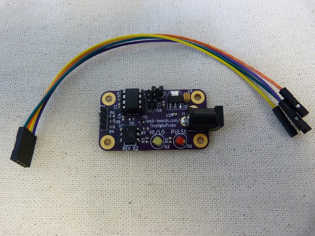
A TinyOptoProbe is a logic probe with an opto-coupled front end. It is useful for probing circuits with floating grounds or cards which do not have accessible grounds. It can also be used as a higher voltage DC logic probe.
Background
Admittedly this is a very strange board. It's not easy to describe where it would be used. In 40 years of working with electronic equipment I have only needed this one time. But, when I needed it, there was no other alternative.
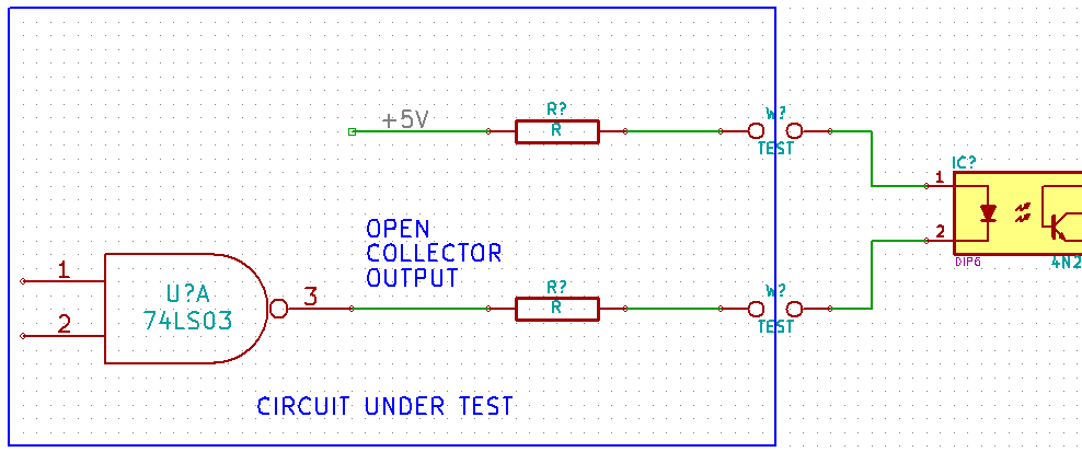
I needed it to debug opto-isolator inputs. I couldn't get to the output that was driving the opto-isolator because it was an a conformal coated card. Add to that the far end was driving the opto-isolator low with an open collector driver. The other side of the source was connected to a resistor pulled up to 5V power. There was no place I could hook a scope since there was no externally accessible ground point. I could probably have attached an LED in place of the opto and watched the light go on and off but what if there was a short pulse which I could not see? I needed an old fashioned logic probe but with a major difference. The logic probe had to be completely isolated from the unit under test and old fashioned logic probes require attaching the the ground. So I came up with the TinyOptoProbe.
This board allows signals to be monitored in an isolated manner from the circuit being monitored. The downside is that it requires 10 mA from the circuit under test to operate. This board is used where measurement of an opto circuit doesn't allow ground clips to be connected to the device under test.
Features
- Isolated Opto-coupled input
- 10 mA nominal input current loop
- All current is returned on the test ground
- No current loop from the Unit Under Test to the logic on the card
- Isolation voltage dependent upon the opto-coupler selected but typically 500 V min
- 5V, 12V, or 24V input levels
- Works with relay circuits for monitoring relay contacts
- Two LEDs (High/Low and Pulse)
- ATTiny85 microproceasor based
- Program to monitor the input and flash the Pulse LED if there is a change (H>L or L>H)
- DC power input
- 9V power
- Can be run from a wall wart power supply or a 9V battery
- Low power consumption, 25 mA max
- 25 mA when both LEDs are on
- 10 mA when one LED is on
- 9V power
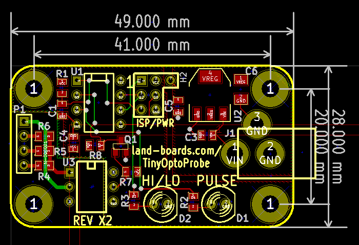
- Small form factor 26x49mm
- (4) 4-40 mounting holes
Operation - Test Opto-Coupler Connection
Disconnect the opto-coupler from the circuit under test Connect power to the DC power jack When the circuit under test is active the HIGH LED will light When there is a change of state the PULSE LED will light
Input Circuit
Layout
Connectors/Headers
H1 VREG power header (X1 board only)
- Install shunt to power card from the DC jack.
- Remove shunt to program Microprocessor from ISP connector (H2).
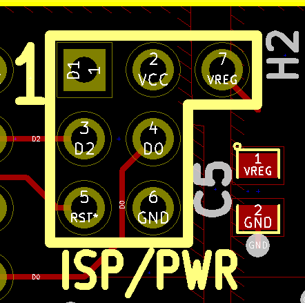
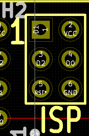
H2 ISP Connector (X2 Board)
This is a strange shaped 7-pin header. This header serves a dual purpose.
- Pin 2 is used for both the ICSP and power select jumpers.
- This effectively prevents the board from being powered by both the ICSP and voltage regulator at the same time.
- If a shunt is installed into pins 2 and 7 the power for the card will come from the voltage regulator on the card.
- Pins 1-6 are the normal pinout for In-Circuit System Programmer (ICSP) pins.
H2 ISP Connector (X1 Board)
J1 - Power Connector
- GND - shell
- +7 to +9V - center pin
P1 - Input Connector
- GND
- +5V
- +12V
- +24V
Software
X2 Improvements over X1
Combined power select jumper and ISP jumper into one part. This prevents the ISP cable and power jumper from being installed at the same time. It is a strange shaped part, but saves board area as well.
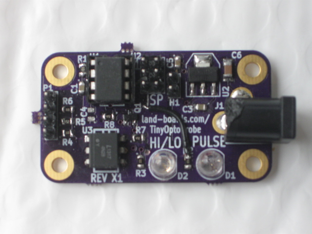
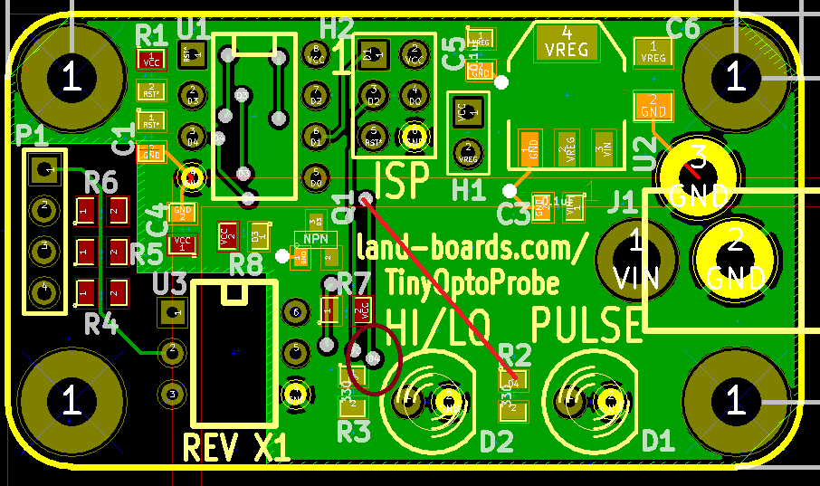
Checkout of Rev X1 CCA
There were a couple significant problems with the X1 circuit card.
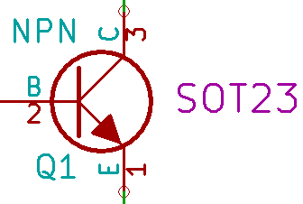
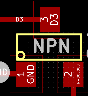
- Transistor Q1 had base and emitter swapped
- Resulted in lack of input signal
- Rework via flipping part over, bending leads down and soldering the part
- Result of rework - input problem fixed
- Must have made a change to the routing of one of the LED lines without running DRC at the end
- Resulted in a power-ground short
- Rework
- Drill out via
- Cut etch
- Add wire
Kicad Schematic SOT23 pinout
Kicad Layout SOT23 pinout
Transistor Datasheet pinout
File:TinyOptoSMT-Transistor-Datasheet-view.PNG
Via drillout, Etch cut and wire add
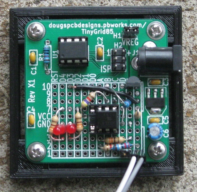
X0 Version of the board
- Built on the TinyGrid85.
