Difference between revisions of "FPGA-ITX-01"
Jump to navigation
Jump to search
Blwikiadmin (talk | contribs) |
Blwikiadmin (talk | contribs) |
||
| (35 intermediate revisions by the same user not shown) | |||
| Line 1: | Line 1: | ||
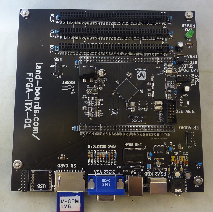
| − | [[FILE:FPGA- | + | [[FILE:FPGA-ITX_P18621_720px.jpg]] |
== Features == | == Features == | ||
| − | * FPGA Adapter Card | + | * FPGA Adapter Card - QMTECH FPGA cards |
| + | ** [[QMTECH Cyclone 10CL006 FPGA Card]] | ||
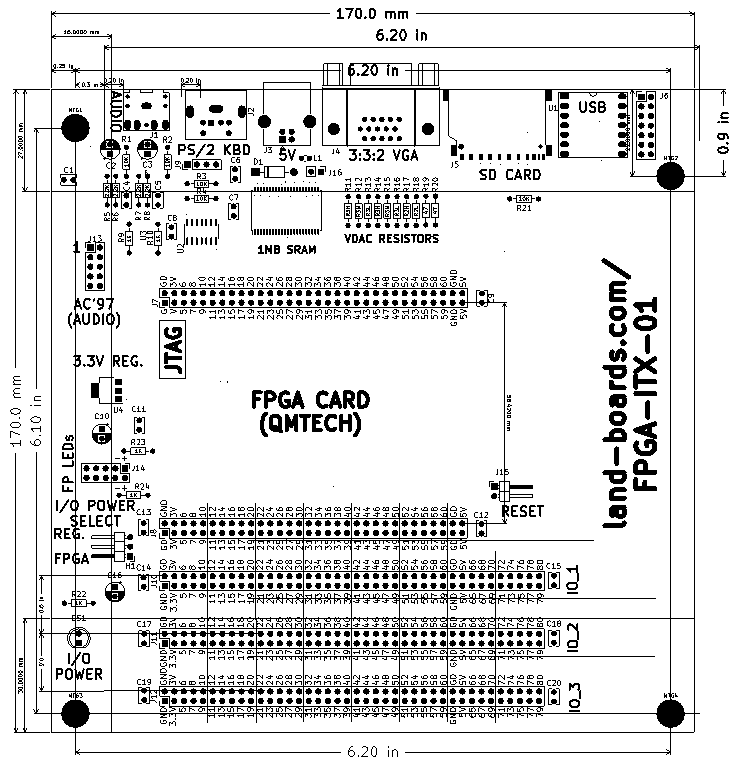
* 170x170mm, Mini-ITX card | * 170x170mm, Mini-ITX card | ||
* 1 MB SRAM | * 1 MB SRAM | ||
* 5V PS/2 keyboard connector | * 5V PS/2 keyboard connector | ||
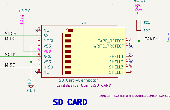
* SD Card socket | * SD Card socket | ||
| − | * 3:3:2 VGA (256 colors | + | * 3:3:2 VGA (256 colors) |
| − | |||
* [[QT_Py_(RP2040_based)|XIAO RP2040]] | * [[QT_Py_(RP2040_based)|XIAO RP2040]] | ||
| + | * Power options, automatically switches between | ||
| + | ** 5V USB B (power only) | ||
| + | ** QTPy USB | ||
| + | ** Used as a USB to Serial converter | ||
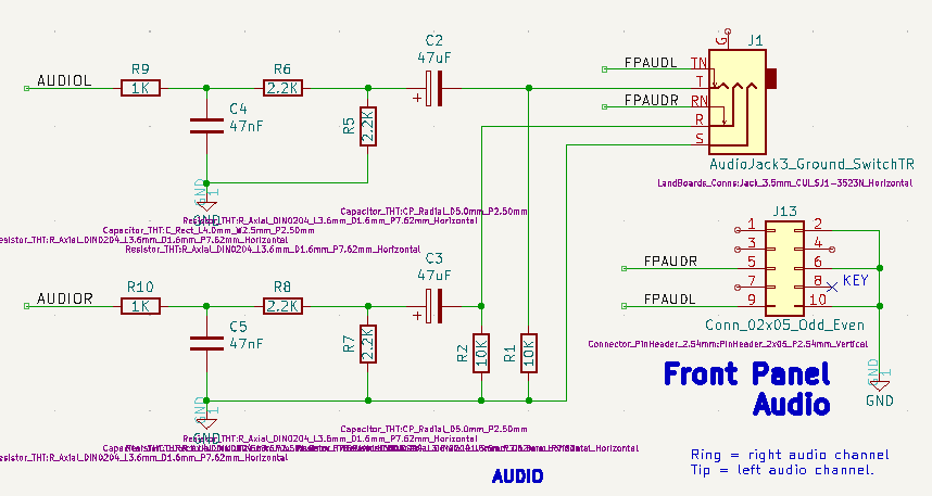
* Stereo Audio Jack | * Stereo Audio Jack | ||
| + | ** PWM Sound Output with Low Pass Filter | ||
* 3 I/O slots | * 3 I/O slots | ||
** Carry all J8 connections | ** Carry all J8 connections | ||
** Slot spacing 0.6" | ** Slot spacing 0.6" | ||
| + | * Current: 130mA with XIAO RP2040 | ||
| + | |||
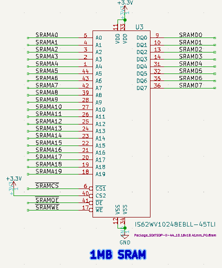
| + | === 1 MB SRAM === | ||
| + | |||
| + | * 1MB SRAM | ||
| + | ** [http://www.issi.com/WW/pdf/62-65WV10248EALL-BLL.pdf IS62WV10248EBLL-45TLI], SRAM. Async, 1Mbx8, 45ns | ||
| + | ** For banked use in CP/M and as RAM Disk in other 8-bit micro designs | ||
| + | |||
| + | [[FILE:RETRO-FPGA-SRAM.PNG]] | ||
== Connectors == | == Connectors == | ||
| Line 72: | Line 86: | ||
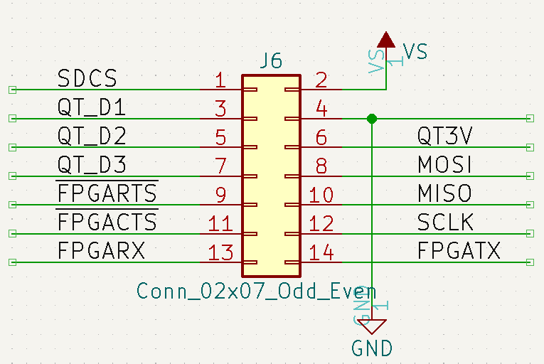
=== J6, U1 - XIAO RP2040 === | === J6, U1 - XIAO RP2040 === | ||
| + | * [[QT_Py_(RP2040_based)|XIAO RP2040]] | ||
| + | * Can power the card from the USB on this card | ||
* All pins are bought out to J1, J2 headers | * All pins are bought out to J1, J2 headers | ||
* Used as an FTDI card replacement | * Used as an FTDI card replacement | ||
| Line 500: | Line 516: | ||
* All pins are usable and are daisy-chained to 3 expansion connectors | * All pins are usable and are daisy-chained to 3 expansion connectors | ||
| − | |||
| − | |||
| − | |||
| − | |||
| − | |||
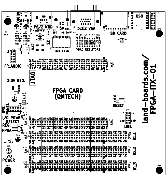
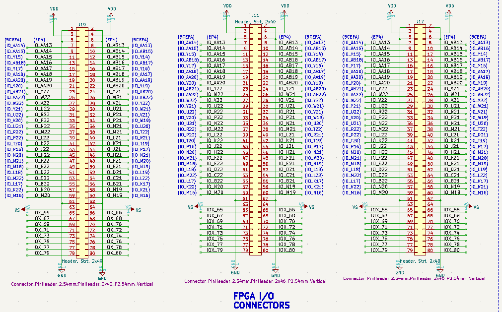
[[file:FPGA-ITX-01_J8.PNG]] | [[file:FPGA-ITX-01_J8.PNG]] | ||
| + | |||
| + | ====== J8 Pins List ====== | ||
| + | |||
| + | * [[QMTECH Cyclone 10CL006 FPGA Card|Cyclone 10 FPGA]] notes | ||
| + | ** Cannot place output or bidirectional pin J8IO[35] or pull-up in input pin location M16 | ||
| + | ** Cannot place output or bidirectional pin J8IO[36] or pull-up in input pin location M15 | ||
| + | ** Cannot place output or bidirectional pin J8IO[57] or pull-up in input pin location E16 | ||
| + | ** Cannot place output or bidirectional pin J8IO[58] or pull-up in input pin location E15 | ||
{| class="wikitable" | {| class="wikitable" | ||
! U8 PIN | ! U8 PIN | ||
| − | ! EP4CE15 | + | ! EP4CE15/55 |
| − | |||
! 5CEFA2 | ! 5CEFA2 | ||
! 10C1006 | ! 10C1006 | ||
! | ! | ||
! U8 PIN | ! U8 PIN | ||
| − | ! EP4CE15 | + | ! EP4CE15/55 |
| − | |||
! 5CEFA2 | ! 5CEFA2 | ||
! 10C1006 | ! 10C1006 | ||
|- | |- | ||
| 1 | | 1 | ||
| − | |||
| GND | | GND | ||
| GND | | GND | ||
| Line 528: | Line 544: | ||
| | | | ||
| 2 | | 2 | ||
| − | |||
| GND | | GND | ||
| GND | | GND | ||
| Line 534: | Line 549: | ||
|- | |- | ||
| 3 | | 3 | ||
| − | |||
| 3.3V | | 3.3V | ||
| 3.3V | | 3.3V | ||
| Line 540: | Line 554: | ||
| | | | ||
| 4 | | 4 | ||
| − | |||
| 3.3V | | 3.3V | ||
| 3.3V | | 3.3V | ||
| Line 546: | Line 559: | ||
|- | |- | ||
| 5 | | 5 | ||
| − | |||
| GND | | GND | ||
| GND | | GND | ||
| Line 552: | Line 564: | ||
| | | | ||
| 6 | | 6 | ||
| − | |||
| GND | | GND | ||
| GND | | GND | ||
| Line 558: | Line 569: | ||
|- | |- | ||
| 7 | | 7 | ||
| − | |||
| PIN_AA13 | | PIN_AA13 | ||
| PIN_AA14 | | PIN_AA14 | ||
| Line 564: | Line 574: | ||
| | | | ||
| 8 | | 8 | ||
| − | |||
| PIN_AB13 | | PIN_AB13 | ||
| PIN_AA13 | | PIN_AA13 | ||
| Line 570: | Line 579: | ||
|- | |- | ||
| 9 | | 9 | ||
| − | |||
| PIN_AA14 | | PIN_AA14 | ||
| PIN_AA15 | | PIN_AA15 | ||
| Line 576: | Line 584: | ||
| | | | ||
| 10 | | 10 | ||
| − | |||
| PIN_AB14 | | PIN_AB14 | ||
| PIN_AB15 | | PIN_AB15 | ||
| Line 582: | Line 589: | ||
|- | |- | ||
| 11 | | 11 | ||
| − | |||
| PIN_AA15 | | PIN_AA15 | ||
| PIN_Y15 | | PIN_Y15 | ||
| Line 588: | Line 594: | ||
| | | | ||
| 12 | | 12 | ||
| − | |||
| PIN_AB15 | | PIN_AB15 | ||
| PIN_Y14 | | PIN_Y14 | ||
| Line 594: | Line 599: | ||
|- | |- | ||
| 13 | | 13 | ||
| − | |||
| PIN_AA16 | | PIN_AA16 | ||
| PIN_AB18 | | PIN_AB18 | ||
| Line 600: | Line 604: | ||
| | | | ||
| 14 | | 14 | ||
| − | |||
| PIN_AB16 | | PIN_AB16 | ||
| PIN_AB17 | | PIN_AB17 | ||
| Line 606: | Line 609: | ||
|- | |- | ||
| 15 | | 15 | ||
| − | |||
| PIN_AA17 | | PIN_AA17 | ||
| PIN_Y17 | | PIN_Y17 | ||
| Line 612: | Line 614: | ||
| | | | ||
| 16 | | 16 | ||
| − | |||
| PIN_AB17 | | PIN_AB17 | ||
| PIN_Y16 | | PIN_Y16 | ||
| Line 618: | Line 619: | ||
|- | |- | ||
| 17 | | 17 | ||
| − | |||
| PIN_AA18 | | PIN_AA18 | ||
| PIN_AA18 | | PIN_AA18 | ||
| Line 624: | Line 624: | ||
| | | | ||
| 18 | | 18 | ||
| − | |||
| PIN_AB18 | | PIN_AB18 | ||
| PIN_AA17 | | PIN_AA17 | ||
| Line 630: | Line 629: | ||
|- | |- | ||
| 19 | | 19 | ||
| − | |||
| PIN_AA19 | | PIN_AA19 | ||
| PIN_AA20 | | PIN_AA20 | ||
| Line 636: | Line 634: | ||
| | | | ||
| 20 | | 20 | ||
| − | |||
| PIN_AB19 | | PIN_AB19 | ||
| PIN_AA19 | | PIN_AA19 | ||
| Line 642: | Line 639: | ||
|- | |- | ||
| 21 | | 21 | ||
| − | |||
| PIN_AA20 | | PIN_AA20 | ||
| PIN_Y20 | | PIN_Y20 | ||
| Line 648: | Line 644: | ||
| | | | ||
| 22 | | 22 | ||
| − | |||
| PIN_AB20 | | PIN_AB20 | ||
| PIN_Y19 | | PIN_Y19 | ||
| Line 654: | Line 649: | ||
|- | |- | ||
| 23 | | 23 | ||
| − | |||
| PIN_Y22 | | PIN_Y22 | ||
| PIN_AB21 | | PIN_AB21 | ||
| Line 660: | Line 654: | ||
| | | | ||
| 24 | | 24 | ||
| − | |||
| PIN_Y21 | | PIN_Y21 | ||
| PIN_AB20 | | PIN_AB20 | ||
| Line 666: | Line 659: | ||
|- | |- | ||
| 25 | | 25 | ||
| − | |||
| PIN_W22 | | PIN_W22 | ||
| PIN_AA22 | | PIN_AA22 | ||
| Line 672: | Line 664: | ||
| | | | ||
| 26 | | 26 | ||
| − | |||
| PIN_W21 | | PIN_W21 | ||
| PIN_AB22 | | PIN_AB22 | ||
| Line 678: | Line 669: | ||
|- | |- | ||
| 27 | | 27 | ||
| − | |||
| PIN_V22 | | PIN_V22 | ||
| PIN_W22 | | PIN_W22 | ||
| Line 684: | Line 674: | ||
| | | | ||
| 28 | | 28 | ||
| − | |||
| PIN_V21 | | PIN_V21 | ||
| PIN_Y22 | | PIN_Y22 | ||
| Line 690: | Line 679: | ||
|- | |- | ||
| 29 | | 29 | ||
| − | |||
| PIN_U22 | | PIN_U22 | ||
| PIN_Y21 | | PIN_Y21 | ||
| Line 696: | Line 684: | ||
| | | | ||
| 30 | | 30 | ||
| − | |||
| PIN_U21 | | PIN_U21 | ||
| PIN_W21 | | PIN_W21 | ||
| Line 702: | Line 689: | ||
|- | |- | ||
| 31 | | 31 | ||
| − | |||
| PIN_R22 | | PIN_R22 | ||
| PIN_U22 | | PIN_U22 | ||
| Line 708: | Line 694: | ||
| | | | ||
| 32 | | 32 | ||
| − | |||
| PIN_R21 | | PIN_R21 | ||
| PIN_V21 | | PIN_V21 | ||
| Line 714: | Line 699: | ||
|- | |- | ||
| 33 | | 33 | ||
| − | |||
| PIN_P22 | | PIN_P22 | ||
| PIN_V20 | | PIN_V20 | ||
| Line 720: | Line 704: | ||
| | | | ||
| 34 | | 34 | ||
| − | |||
| PIN_P21 | | PIN_P21 | ||
| PIN_W19 | | PIN_W19 | ||
| Line 726: | Line 709: | ||
|- | |- | ||
| 35 | | 35 | ||
| − | |||
| PIN_N22 | | PIN_N22 | ||
| PIN_U21 | | PIN_U21 | ||
| Line 732: | Line 714: | ||
| | | | ||
| 36 | | 36 | ||
| − | |||
| PIN_N21 | | PIN_N21 | ||
| PIN_U20 | | PIN_U20 | ||
| Line 738: | Line 719: | ||
|- | |- | ||
| 37 | | 37 | ||
| − | |||
| PIN_M22 | | PIN_M22 | ||
| PIN_R22 | | PIN_R22 | ||
| Line 744: | Line 724: | ||
| | | | ||
| 38 | | 38 | ||
| − | |||
| PIN_M21 | | PIN_M21 | ||
| PIN_T22 | | PIN_T22 | ||
| Line 750: | Line 729: | ||
|- | |- | ||
| 39 | | 39 | ||
| − | |||
| PIN_L22 | | PIN_L22 | ||
| PIN_P22 | | PIN_P22 | ||
| Line 756: | Line 734: | ||
| | | | ||
| 40 | | 40 | ||
| − | |||
| PIN_L21 | | PIN_L21 | ||
| PIN_R21 | | PIN_R21 | ||
| Line 762: | Line 739: | ||
|- | |- | ||
| 41 | | 41 | ||
| − | |||
| PIN_K22 | | PIN_K22 | ||
| PIN_T20 | | PIN_T20 | ||
| Line 768: | Line 744: | ||
| | | | ||
| 42 | | 42 | ||
| − | |||
| PIN_K21 | | PIN_K21 | ||
| PIN_T19 | | PIN_T19 | ||
| Line 774: | Line 749: | ||
|- | |- | ||
| 43 | | 43 | ||
| − | |||
| PIN_J22 | | PIN_J22 | ||
| PIN_P16 | | PIN_P16 | ||
| Line 780: | Line 754: | ||
| | | | ||
| 44 | | 44 | ||
| − | |||
| PIN_J21 | | PIN_J21 | ||
| PIN_P17 | | PIN_P17 | ||
| Line 786: | Line 759: | ||
|- | |- | ||
| 45 | | 45 | ||
| − | |||
| PIN_H22 | | PIN_H22 | ||
| PIN_N20 | | PIN_N20 | ||
| Line 792: | Line 764: | ||
| | | | ||
| 46 | | 46 | ||
| − | |||
| PIN_H21 | | PIN_H21 | ||
| PIN_N21 | | PIN_N21 | ||
| Line 798: | Line 769: | ||
|- | |- | ||
| 47 | | 47 | ||
| − | |||
| PIN_F22 | | PIN_F22 | ||
| PIN_M21 | | PIN_M21 | ||
| Line 804: | Line 774: | ||
| | | | ||
| 48 | | 48 | ||
| − | |||
| PIN_F21 | | PIN_F21 | ||
| PIN_M20 | | PIN_M20 | ||
| Line 810: | Line 779: | ||
|- | |- | ||
| 49 | | 49 | ||
| − | |||
| PIN_E22 | | PIN_E22 | ||
| PIN_M18 | | PIN_M18 | ||
| Line 816: | Line 784: | ||
| | | | ||
| 50 | | 50 | ||
| − | |||
| PIN_E21 | | PIN_E21 | ||
| PIN_N19 | | PIN_N19 | ||
| Line 822: | Line 789: | ||
|- | |- | ||
| 51 | | 51 | ||
| − | |||
| PIN_D22 | | PIN_D22 | ||
| PIN_L18 | | PIN_L18 | ||
| Line 828: | Line 794: | ||
| | | | ||
| 52 | | 52 | ||
| − | |||
| PIN_D21 | | PIN_D21 | ||
| PIN_L19 | | PIN_L19 | ||
| Line 834: | Line 799: | ||
|- | |- | ||
| 53 | | 53 | ||
| − | |||
| PIN_C22 | | PIN_C22 | ||
| PIN_M22 | | PIN_M22 | ||
| Line 840: | Line 804: | ||
| | | | ||
| 54 | | 54 | ||
| − | |||
| PIN_C21 | | PIN_C21 | ||
| PIN_L22 | | PIN_L22 | ||
| Line 846: | Line 809: | ||
|- | |- | ||
| 55 | | 55 | ||
| − | |||
| PIN_B22 | | PIN_B22 | ||
| PIN_L17 | | PIN_L17 | ||
| Line 852: | Line 814: | ||
| | | | ||
| 56 | | 56 | ||
| − | |||
| PIN_B21 | | PIN_B21 | ||
| PIN_K17 | | PIN_K17 | ||
| Line 858: | Line 819: | ||
|- | |- | ||
| 57 | | 57 | ||
| − | |||
| PIN_N20 | | PIN_N20 | ||
| PIN_K22 | | PIN_K22 | ||
| Line 864: | Line 824: | ||
| | | | ||
| 58 | | 58 | ||
| − | |||
| PIN_N19 | | PIN_N19 | ||
| PIN_K21 | | PIN_K21 | ||
| Line 870: | Line 829: | ||
|- | |- | ||
| 59 | | 59 | ||
| − | |||
| PIN_M20 | | PIN_M20 | ||
| PIN_M16 | | PIN_M16 | ||
| Line 876: | Line 834: | ||
| | | | ||
| 60 | | 60 | ||
| − | |||
| PIN_M19 | | PIN_M19 | ||
| PIN_N16 | | PIN_N16 | ||
| Line 882: | Line 839: | ||
|- | |- | ||
| 61 | | 61 | ||
| − | |||
| GND | | GND | ||
| GND | | GND | ||
| Line 888: | Line 844: | ||
| | | | ||
| 62 | | 62 | ||
| − | |||
| GND | | GND | ||
| GND | | GND | ||
| Line 894: | Line 849: | ||
|- | |- | ||
| 63 | | 63 | ||
| − | |||
| 5V | | 5V | ||
| 5V | | 5V | ||
| Line 900: | Line 854: | ||
| | | | ||
| 64 | | 64 | ||
| − | |||
| 5V | | 5V | ||
| 5V | | 5V | ||
| Line 920: | Line 873: | ||
[[file:FPGA-ITX-01_J10-J12_IO_Conns.PNG]] | [[file:FPGA-ITX-01_J10-J12_IO_Conns.PNG]] | ||
| + | |||
| + | ==== J10-J12 Pins List ==== | ||
{| class="wikitable" | {| class="wikitable" | ||
! U8 PIN | ! U8 PIN | ||
| − | ! EP4CE15 | + | ! EP4CE15/55 |
| − | |||
! 5CEFA2 | ! 5CEFA2 | ||
! 10C1006 | ! 10C1006 | ||
! | ! | ||
! U8 PIN | ! U8 PIN | ||
| − | ! EP4CE15 | + | ! EP4CE15/55 |
| − | |||
! 5CEFA2 | ! 5CEFA2 | ||
! 10C1006 | ! 10C1006 | ||
|- | |- | ||
| 1 | | 1 | ||
| − | |||
| GND | | GND | ||
| GND | | GND | ||
| Line 941: | Line 893: | ||
| | | | ||
| 2 | | 2 | ||
| − | |||
| GND | | GND | ||
| GND | | GND | ||
| Line 947: | Line 898: | ||
|- | |- | ||
| 3 | | 3 | ||
| − | |||
| 3.3V | | 3.3V | ||
| 3.3V | | 3.3V | ||
| Line 953: | Line 903: | ||
| | | | ||
| 4 | | 4 | ||
| − | |||
| 3.3V | | 3.3V | ||
| 3.3V | | 3.3V | ||
| Line 959: | Line 908: | ||
|- | |- | ||
| 5 | | 5 | ||
| − | |||
| GND | | GND | ||
| GND | | GND | ||
| Line 965: | Line 913: | ||
| | | | ||
| 6 | | 6 | ||
| − | |||
| GND | | GND | ||
| GND | | GND | ||
| Line 971: | Line 918: | ||
|- | |- | ||
| 7 | | 7 | ||
| − | |||
| PIN_AA13 | | PIN_AA13 | ||
| PIN_AA14 | | PIN_AA14 | ||
| Line 977: | Line 923: | ||
| | | | ||
| 8 | | 8 | ||
| − | |||
| PIN_AB13 | | PIN_AB13 | ||
| PIN_AA13 | | PIN_AA13 | ||
| Line 983: | Line 928: | ||
|- | |- | ||
| 9 | | 9 | ||
| − | |||
| PIN_AA14 | | PIN_AA14 | ||
| PIN_AA15 | | PIN_AA15 | ||
| Line 989: | Line 933: | ||
| | | | ||
| 10 | | 10 | ||
| − | |||
| PIN_AB14 | | PIN_AB14 | ||
| PIN_AB15 | | PIN_AB15 | ||
| Line 995: | Line 938: | ||
|- | |- | ||
| 11 | | 11 | ||
| − | |||
| PIN_AA15 | | PIN_AA15 | ||
| PIN_Y15 | | PIN_Y15 | ||
| Line 1,001: | Line 943: | ||
| | | | ||
| 12 | | 12 | ||
| − | |||
| PIN_AB15 | | PIN_AB15 | ||
| PIN_Y14 | | PIN_Y14 | ||
| Line 1,007: | Line 948: | ||
|- | |- | ||
| 13 | | 13 | ||
| − | |||
| PIN_AA16 | | PIN_AA16 | ||
| PIN_AB18 | | PIN_AB18 | ||
| Line 1,013: | Line 953: | ||
| | | | ||
| 14 | | 14 | ||
| − | |||
| PIN_AB16 | | PIN_AB16 | ||
| PIN_AB17 | | PIN_AB17 | ||
| Line 1,019: | Line 958: | ||
|- | |- | ||
| 15 | | 15 | ||
| − | |||
| PIN_AA17 | | PIN_AA17 | ||
| PIN_Y17 | | PIN_Y17 | ||
| Line 1,025: | Line 963: | ||
| | | | ||
| 16 | | 16 | ||
| − | |||
| PIN_AB17 | | PIN_AB17 | ||
| PIN_Y16 | | PIN_Y16 | ||
| Line 1,031: | Line 968: | ||
|- | |- | ||
| 17 | | 17 | ||
| − | |||
| PIN_AA18 | | PIN_AA18 | ||
| PIN_AA18 | | PIN_AA18 | ||
| Line 1,037: | Line 973: | ||
| | | | ||
| 18 | | 18 | ||
| − | |||
| PIN_AB18 | | PIN_AB18 | ||
| PIN_AA17 | | PIN_AA17 | ||
| Line 1,043: | Line 978: | ||
|- | |- | ||
| 19 | | 19 | ||
| − | |||
| PIN_AA19 | | PIN_AA19 | ||
| PIN_AA20 | | PIN_AA20 | ||
| Line 1,049: | Line 983: | ||
| | | | ||
| 20 | | 20 | ||
| − | |||
| PIN_AB19 | | PIN_AB19 | ||
| PIN_AA19 | | PIN_AA19 | ||
| Line 1,055: | Line 988: | ||
|- | |- | ||
| 21 | | 21 | ||
| − | |||
| PIN_AA20 | | PIN_AA20 | ||
| PIN_Y20 | | PIN_Y20 | ||
| Line 1,061: | Line 993: | ||
| | | | ||
| 22 | | 22 | ||
| − | |||
| PIN_AB20 | | PIN_AB20 | ||
| PIN_Y19 | | PIN_Y19 | ||
| Line 1,067: | Line 998: | ||
|- | |- | ||
| 23 | | 23 | ||
| − | |||
| PIN_Y22 | | PIN_Y22 | ||
| PIN_AB21 | | PIN_AB21 | ||
| Line 1,073: | Line 1,003: | ||
| | | | ||
| 24 | | 24 | ||
| − | |||
| PIN_Y21 | | PIN_Y21 | ||
| PIN_AB20 | | PIN_AB20 | ||
| Line 1,079: | Line 1,008: | ||
|- | |- | ||
| 25 | | 25 | ||
| − | |||
| PIN_W22 | | PIN_W22 | ||
| PIN_AA22 | | PIN_AA22 | ||
| Line 1,085: | Line 1,013: | ||
| | | | ||
| 26 | | 26 | ||
| − | |||
| PIN_W21 | | PIN_W21 | ||
| PIN_AB22 | | PIN_AB22 | ||
| Line 1,091: | Line 1,018: | ||
|- | |- | ||
| 27 | | 27 | ||
| − | |||
| PIN_V22 | | PIN_V22 | ||
| PIN_W22 | | PIN_W22 | ||
| Line 1,097: | Line 1,023: | ||
| | | | ||
| 28 | | 28 | ||
| − | |||
| PIN_V21 | | PIN_V21 | ||
| PIN_Y22 | | PIN_Y22 | ||
| Line 1,103: | Line 1,028: | ||
|- | |- | ||
| 29 | | 29 | ||
| − | |||
| PIN_U22 | | PIN_U22 | ||
| PIN_Y21 | | PIN_Y21 | ||
| Line 1,109: | Line 1,033: | ||
| | | | ||
| 30 | | 30 | ||
| − | |||
| PIN_U21 | | PIN_U21 | ||
| PIN_W21 | | PIN_W21 | ||
| Line 1,115: | Line 1,038: | ||
|- | |- | ||
| 31 | | 31 | ||
| − | |||
| PIN_R22 | | PIN_R22 | ||
| PIN_U22 | | PIN_U22 | ||
| Line 1,121: | Line 1,043: | ||
| | | | ||
| 32 | | 32 | ||
| − | |||
| PIN_R21 | | PIN_R21 | ||
| PIN_V21 | | PIN_V21 | ||
| Line 1,127: | Line 1,048: | ||
|- | |- | ||
| 33 | | 33 | ||
| − | |||
| PIN_P22 | | PIN_P22 | ||
| PIN_V20 | | PIN_V20 | ||
| Line 1,133: | Line 1,053: | ||
| | | | ||
| 34 | | 34 | ||
| − | |||
| PIN_P21 | | PIN_P21 | ||
| PIN_W19 | | PIN_W19 | ||
| Line 1,139: | Line 1,058: | ||
|- | |- | ||
| 35 | | 35 | ||
| − | |||
| PIN_N22 | | PIN_N22 | ||
| PIN_U21 | | PIN_U21 | ||
| Line 1,145: | Line 1,063: | ||
| | | | ||
| 36 | | 36 | ||
| − | |||
| PIN_N21 | | PIN_N21 | ||
| PIN_U20 | | PIN_U20 | ||
| Line 1,151: | Line 1,068: | ||
|- | |- | ||
| 37 | | 37 | ||
| − | |||
| PIN_M22 | | PIN_M22 | ||
| PIN_R22 | | PIN_R22 | ||
| Line 1,157: | Line 1,073: | ||
| | | | ||
| 38 | | 38 | ||
| − | |||
| PIN_M21 | | PIN_M21 | ||
| PIN_T22 | | PIN_T22 | ||
| Line 1,163: | Line 1,078: | ||
|- | |- | ||
| 39 | | 39 | ||
| − | |||
| PIN_L22 | | PIN_L22 | ||
| PIN_P22 | | PIN_P22 | ||
| Line 1,169: | Line 1,083: | ||
| | | | ||
| 40 | | 40 | ||
| − | |||
| PIN_L21 | | PIN_L21 | ||
| PIN_R21 | | PIN_R21 | ||
| Line 1,175: | Line 1,088: | ||
|- | |- | ||
| 41 | | 41 | ||
| − | |||
| PIN_K22 | | PIN_K22 | ||
| PIN_T20 | | PIN_T20 | ||
| Line 1,181: | Line 1,093: | ||
| | | | ||
| 42 | | 42 | ||
| − | |||
| PIN_K21 | | PIN_K21 | ||
| PIN_T19 | | PIN_T19 | ||
| Line 1,187: | Line 1,098: | ||
|- | |- | ||
| 43 | | 43 | ||
| − | |||
| PIN_J22 | | PIN_J22 | ||
| PIN_P16 | | PIN_P16 | ||
| Line 1,193: | Line 1,103: | ||
| | | | ||
| 44 | | 44 | ||
| − | |||
| PIN_J21 | | PIN_J21 | ||
| PIN_P17 | | PIN_P17 | ||
| Line 1,199: | Line 1,108: | ||
|- | |- | ||
| 45 | | 45 | ||
| − | |||
| PIN_H22 | | PIN_H22 | ||
| PIN_N20 | | PIN_N20 | ||
| Line 1,205: | Line 1,113: | ||
| | | | ||
| 46 | | 46 | ||
| − | |||
| PIN_H21 | | PIN_H21 | ||
| PIN_N21 | | PIN_N21 | ||
| Line 1,211: | Line 1,118: | ||
|- | |- | ||
| 47 | | 47 | ||
| − | |||
| PIN_F22 | | PIN_F22 | ||
| PIN_M21 | | PIN_M21 | ||
| Line 1,217: | Line 1,123: | ||
| | | | ||
| 48 | | 48 | ||
| − | |||
| PIN_F21 | | PIN_F21 | ||
| PIN_M20 | | PIN_M20 | ||
| Line 1,223: | Line 1,128: | ||
|- | |- | ||
| 49 | | 49 | ||
| − | |||
| PIN_E22 | | PIN_E22 | ||
| PIN_M18 | | PIN_M18 | ||
| Line 1,229: | Line 1,133: | ||
| | | | ||
| 50 | | 50 | ||
| − | |||
| PIN_E21 | | PIN_E21 | ||
| PIN_N19 | | PIN_N19 | ||
| Line 1,235: | Line 1,138: | ||
|- | |- | ||
| 51 | | 51 | ||
| − | |||
| PIN_D22 | | PIN_D22 | ||
| PIN_L18 | | PIN_L18 | ||
| Line 1,241: | Line 1,143: | ||
| | | | ||
| 52 | | 52 | ||
| − | |||
| PIN_D21 | | PIN_D21 | ||
| PIN_L19 | | PIN_L19 | ||
| Line 1,247: | Line 1,148: | ||
|- | |- | ||
| 53 | | 53 | ||
| − | |||
| PIN_C22 | | PIN_C22 | ||
| PIN_M22 | | PIN_M22 | ||
| Line 1,253: | Line 1,153: | ||
| | | | ||
| 54 | | 54 | ||
| − | |||
| PIN_C21 | | PIN_C21 | ||
| PIN_L22 | | PIN_L22 | ||
| Line 1,259: | Line 1,158: | ||
|- | |- | ||
| 55 | | 55 | ||
| − | |||
| PIN_B22 | | PIN_B22 | ||
| PIN_L17 | | PIN_L17 | ||
| Line 1,265: | Line 1,163: | ||
| | | | ||
| 56 | | 56 | ||
| − | |||
| PIN_B21 | | PIN_B21 | ||
| PIN_K17 | | PIN_K17 | ||
| Line 1,271: | Line 1,168: | ||
|- | |- | ||
| 57 | | 57 | ||
| − | |||
| PIN_N20 | | PIN_N20 | ||
| PIN_K22 | | PIN_K22 | ||
| Line 1,277: | Line 1,173: | ||
| | | | ||
| 58 | | 58 | ||
| − | |||
| PIN_N19 | | PIN_N19 | ||
| PIN_K21 | | PIN_K21 | ||
| Line 1,283: | Line 1,178: | ||
|- | |- | ||
| 59 | | 59 | ||
| − | |||
| PIN_M20 | | PIN_M20 | ||
| PIN_M16 | | PIN_M16 | ||
| Line 1,289: | Line 1,183: | ||
| | | | ||
| 60 | | 60 | ||
| − | |||
| PIN_M19 | | PIN_M19 | ||
| PIN_N16 | | PIN_N16 | ||
| Line 1,295: | Line 1,188: | ||
|- | |- | ||
| 61 | | 61 | ||
| − | |||
| GND | | GND | ||
| GND | | GND | ||
| Line 1,301: | Line 1,193: | ||
| | | | ||
| 62 | | 62 | ||
| − | |||
| GND | | GND | ||
| GND | | GND | ||
| Line 1,307: | Line 1,198: | ||
|- | |- | ||
| 63 | | 63 | ||
| − | |||
| 5V | | 5V | ||
| 5V | | 5V | ||
| Line 1,313: | Line 1,203: | ||
| | | | ||
| 64 | | 64 | ||
| − | |||
| 5V | | 5V | ||
| 5V | | 5V | ||
| Line 1,319: | Line 1,208: | ||
|- | |- | ||
| 65 | | 65 | ||
| − | |||
| IOX_65 | | IOX_65 | ||
| IOX_65 | | IOX_65 | ||
| Line 1,325: | Line 1,213: | ||
| | | | ||
| 66 | | 66 | ||
| − | |||
| IOX_66 | | IOX_66 | ||
| IOX_66 | | IOX_66 | ||
| Line 1,331: | Line 1,218: | ||
|- | |- | ||
| 67 | | 67 | ||
| − | |||
| IOX_67 | | IOX_67 | ||
| IOX_67 | | IOX_67 | ||
| Line 1,337: | Line 1,223: | ||
| | | | ||
| 68 | | 68 | ||
| − | |||
| IOX_68 | | IOX_68 | ||
| IOX_68 | | IOX_68 | ||
| Line 1,343: | Line 1,228: | ||
|- | |- | ||
| 69 | | 69 | ||
| − | |||
| IOX_69 | | IOX_69 | ||
| IOX_69 | | IOX_69 | ||
| Line 1,349: | Line 1,233: | ||
| | | | ||
| 70 | | 70 | ||
| − | |||
| IOX_70 | | IOX_70 | ||
| IOX_70 | | IOX_70 | ||
| Line 1,355: | Line 1,238: | ||
|- | |- | ||
| 71 | | 71 | ||
| − | |||
| IOX_71 | | IOX_71 | ||
| IOX_71 | | IOX_71 | ||
| Line 1,361: | Line 1,243: | ||
| | | | ||
| 72 | | 72 | ||
| − | |||
| IOX_72 | | IOX_72 | ||
| IOX_72 | | IOX_72 | ||
| Line 1,367: | Line 1,248: | ||
|- | |- | ||
| 73 | | 73 | ||
| − | |||
| IOX_73 | | IOX_73 | ||
| IOX_73 | | IOX_73 | ||
| Line 1,373: | Line 1,253: | ||
| | | | ||
| 74 | | 74 | ||
| − | |||
| IOX_74 | | IOX_74 | ||
| IOX_74 | | IOX_74 | ||
| Line 1,379: | Line 1,258: | ||
|- | |- | ||
| 75 | | 75 | ||
| − | |||
| IOX_75 | | IOX_75 | ||
| IOX_75 | | IOX_75 | ||
| Line 1,385: | Line 1,263: | ||
| | | | ||
| 76 | | 76 | ||
| − | |||
| IOX_76 | | IOX_76 | ||
| IOX_76 | | IOX_76 | ||
| Line 1,391: | Line 1,268: | ||
|- | |- | ||
| 77 | | 77 | ||
| − | |||
| IOX_77 | | IOX_77 | ||
| IOX_77 | | IOX_77 | ||
| Line 1,397: | Line 1,273: | ||
| | | | ||
| 78 | | 78 | ||
| − | |||
| IOX_78 | | IOX_78 | ||
| IOX_78 | | IOX_78 | ||
| Line 1,403: | Line 1,278: | ||
|- | |- | ||
| 79 | | 79 | ||
| − | |||
| IOX_79 | | IOX_79 | ||
| IOX_79 | | IOX_79 | ||
| Line 1,412: | Line 1,286: | ||
| IOX_80 | | IOX_80 | ||
| IOX_80 | | IOX_80 | ||
| − | | | + | |- |
| + | | | ||
| + | | IOX_81 | ||
| + | | IOX_81 | ||
| + | | IOX_81 | ||
| + | | | ||
| + | | 82 | ||
| + | | IOX_82 | ||
| + | | IOX_82 | ||
| + | | IOX_82 | ||
|- | |- | ||
|} | |} | ||
| Line 1,436: | Line 1,319: | ||
* Can use 3.3V from FPGA card or on-board 3.3V regulator | * Can use 3.3V from FPGA card or on-board 3.3V regulator | ||
| − | |||
| − | |||
| − | |||
| − | |||
| − | |||
| − | |||
| − | |||
| − | |||
== 170x170mm, Mini-ITX card == | == 170x170mm, Mini-ITX card == | ||
| Line 1,479: | Line 1,354: | ||
FPGA-ITX-01 expansion cards plug into the expansion connectors to expand the functionality of the FPGA design. | FPGA-ITX-01 expansion cards plug into the expansion connectors to expand the functionality of the FPGA design. | ||
| − | === | + | === ITX-65C816 === |
| − | 65C816 CPU module. | + | * [[ITX-65C816]] |
| + | * W65C816 CPU module | ||
| + | ** 3.3V | ||
| + | ** Running at 8.33 MHz | ||
| + | ** Native mode (65C816 extended code) and emulation mode (65C02 code) | ||
| + | ** Native mode allows for 24-bit address space | ||
| − | [[file:ITX- | + | [[file:ITX-65816_P18616_720PX.jpg]] |
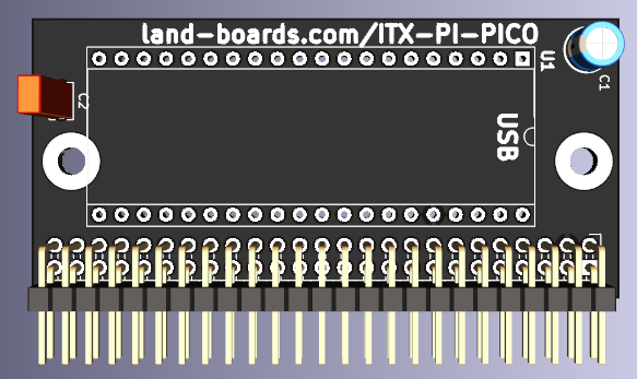
| − | === | + | === ITX-PI-PICO === |
| + | * [[ITX-PI-PICO]] | ||
* Raspberry Pi Pico Module | * Raspberry Pi Pico Module | ||
[[file:ITX-Pi-PICO_FRONT_3D.png]] | [[file:ITX-Pi-PICO_FRONT_3D.png]] | ||
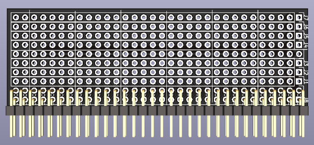
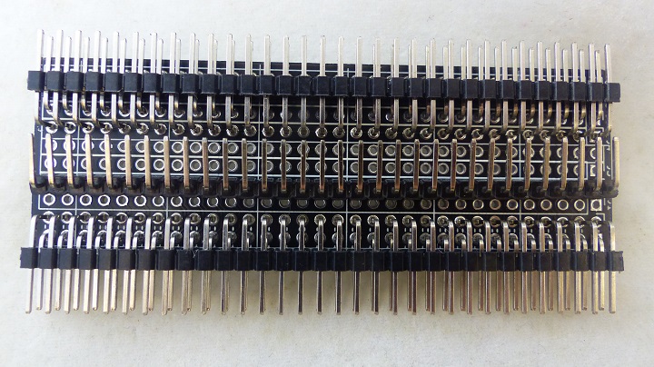
| − | === | + | === ITX-BKOUT === |
| + | * [[ITX-BKOUT]] | ||
* Breakout card which connects to the pins of the expansion connectors with power/ground down the center of the card. | * Breakout card which connects to the pins of the expansion connectors with power/ground down the center of the card. | ||
[[file:ITX-BKOUT_FRONT_3D.PNG]] | [[file:ITX-BKOUT_FRONT_3D.PNG]] | ||
| − | + | * Configured as Bus Monitor for Logic Analyzer | |
| + | [[file:ITX-BKOUT_P18619_720px.jpg]] | ||
| + | |||
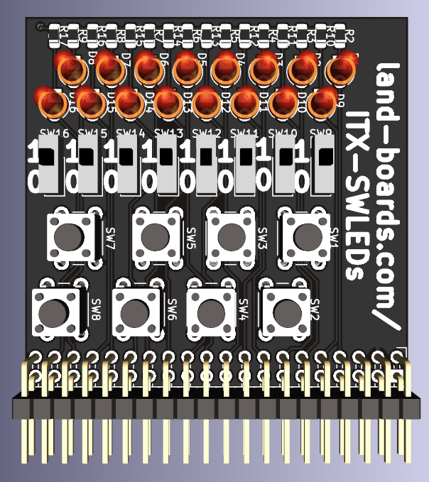
| + | === ITX-SWLEDs === | ||
| + | |||
| + | * [[ITX-SWLEDs]] | ||
* 8 pushbuttons, 8 slide switches, 16 LEDs. | * 8 pushbuttons, 8 slide switches, 16 LEDs. | ||
| Line 1,511: | Line 1,398: | ||
[[FILE:QMTECH_FPGA_EP4CE15.jpg]] | [[FILE:QMTECH_FPGA_EP4CE15.jpg]] | ||
| − | == Multicomp Builds == | + | == Software == |
| + | |||
| + | Software that runs on the card | ||
| + | |||
| + | === Multicomp Builds === | ||
Tested Multicomp builds | Tested Multicomp builds | ||
| Line 1,521: | Line 1,412: | ||
* [https://github.com/douggilliland/MultiComp/tree/master/MultiComp_On_FPGA-ITX-01/Multicomp-MPM Multicomp-MPM] | * [https://github.com/douggilliland/MultiComp/tree/master/MultiComp_On_FPGA-ITX-01/Multicomp-MPM Multicomp-MPM] | ||
* [https://github.com/douggilliland/MultiComp/tree/master/MultiComp_On_FPGA-ITX-01/UK101_41K UK101_41K] | * [https://github.com/douggilliland/MultiComp/tree/master/MultiComp_On_FPGA-ITX-01/UK101_41K UK101_41K] | ||
| + | |||
| + | === XIAO RP2040 === | ||
| + | |||
| + | * [https://github.com/land-boards/lb-Arduino-Code/tree/master/LBCards/FPGA-ITX/USB_SERIAL USB-SERIAL] - Arduino sketch turns the RP2040 into a USB to Serial Bridge | ||
| + | ** Runs at 115,200 baud | ||
| + | ** Hardware Handshake implemented | ||
| + | *** Only uses RTS output from the FPGA to hold off output | ||
| + | ** Most Multicomp builds switch I/O with F1 key | ||
| + | * TeraTerm at 115,200 baud | ||
== Revision History == | == Revision History == | ||
| Line 1,535: | Line 1,435: | ||
* Added Rev 2 marking | * Added Rev 2 marking | ||
* Change R2H, etc to call out R/G/B (match PL) | * Change R2H, etc to call out R/G/B (match PL) | ||
| − | |||
| − | |||
| − | |||
| − | |||
| − | |||
=== Rev 1 === | === Rev 1 === | ||
| − | * Upper right mounting hole is in wrong spot | + | * Upper right mounting hole (near XAIO USB/Serial interface) is in wrong spot |
** At 0.9" from edge, should be 0.9" from upper left mounting hole | ** At 0.9" from edge, should be 0.9" from upper left mounting hole | ||
| − | ** Not big issue, no mechanical interference on board, just use 3 mounting holes | + | ** Not big issue, no mechanical interference on board, just use 3 mounting holes to install in case |
| − | * Yabs = 2.47480315, change to 2.87480315 | + | ** Yabs = 2.47480315, change to 2.87480315 |
* R23 DRC error | * R23 DRC error | ||
** Overshot pin on rear side | ** Overshot pin on rear side | ||
** Verified right pin is connected | ** Verified right pin is connected | ||
| − | * Input only pins do not support internal pull-ups | + | * Input only pins (using Cyclone 10) do not support internal pull-ups |
* Missing Rev marking (use P-Touch label) | * Missing Rev marking (use P-Touch label) | ||
| + | * Tested/works | ||
| + | ** Video | ||
| + | ** PS/2 keyboard | ||
| + | ** SD card | ||
| + | ** 5V input | ||
== Assembly Sheet == | == Assembly Sheet == | ||
* [[FPGA-ITX-01 Rev 1 Assembly Sheet]] | * [[FPGA-ITX-01 Rev 1 Assembly Sheet]] | ||
Latest revision as of 15:12, 24 May 2023
Contents
- 1 Features
- 2 Connectors
- 2.1 J1, J13 - Stereo Audio Jack
- 2.2 J2, J9 - 5V PS/2 keyboard connector
- 2.3 J3 - 5V USB B (power only)
- 2.4 J4 - 3:3:2 VGA (256 colors
- 2.5 J5 - SD Card socket
- 2.6 J6, U1 - XIAO RP2040
- 2.7 J7, J8 - FPGA Adapter Card
- 2.8 J10-J12 - 3 I/O slots IO_1-IO_3
- 2.9 J14 - Power LEDs
- 2.10 J15 - Reset Switch
- 2.11 J16 - Power Switch
- 2.12 H1 - I/O Slots Power Select Jumper
- 3 170x170mm, Mini-ITX card
- 4 Expansion Cards
- 5 Mechanicals
- 6 Software
- 7 Revision History
- 8 Assembly Sheet
Features
- FPGA Adapter Card - QMTECH FPGA cards
- 170x170mm, Mini-ITX card
- 1 MB SRAM
- 5V PS/2 keyboard connector
- SD Card socket
- 3:3:2 VGA (256 colors)
- XIAO RP2040
- Power options, automatically switches between
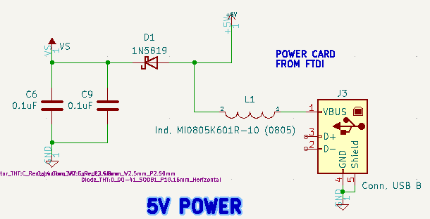
- 5V USB B (power only)
- QTPy USB
- Used as a USB to Serial converter
- Stereo Audio Jack
- PWM Sound Output with Low Pass Filter
- 3 I/O slots
- Carry all J8 connections
- Slot spacing 0.6"
- Current: 130mA with XIAO RP2040
1 MB SRAM
- 1MB SRAM
- IS62WV10248EBLL-45TLI, SRAM. Async, 1Mbx8, 45ns
- For banked use in CP/M and as RAM Disk in other 8-bit micro designs
Connectors
J1, J13 - Stereo Audio Jack
- 3.5mm stereo connector
- Jack on card has priority over connection to chassis jack
- Chassis front panel jack gets disconnected when jack is plugged into the card
- Stereo pinout
- Tip: This acts as the left channel signal wire
- Ring: This acts as the right channel signal wire
- Sleeve: This acts as the common return wire
- J13 is header to case jack
- Minimal LP filter
- FPGA Sound on our GitHub
- Using PWM to generate sound
- How to Generate Sound using PWM
- Run at frequency well above audio, say 44.1 or 48 KHz
- Output of filter with 50% duty cycle will produce smoothed average voltage at the mid-point
- Values > 50% duty cycle will produce a voltage higher than the average
- Values < 50% duty cycle will produce a voltage lower than the average
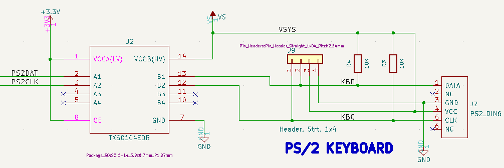
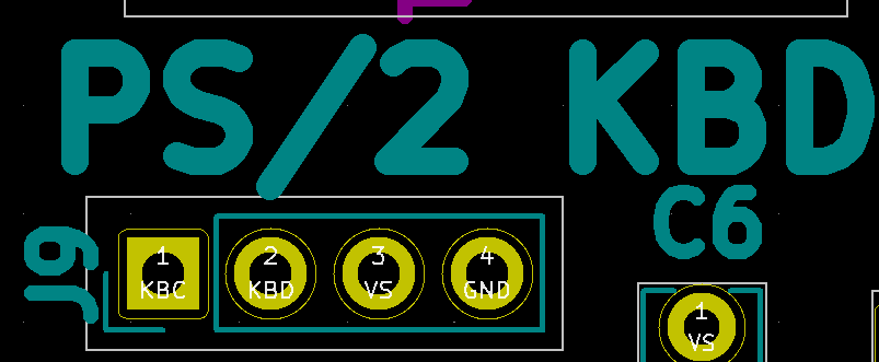
J2, J9 - 5V PS/2 keyboard connector
- PS/2 connector
- 5V to 3.3V level shifter
- CLK
- DATA
- +5V
- GND
J3 - 5V USB B (power only)
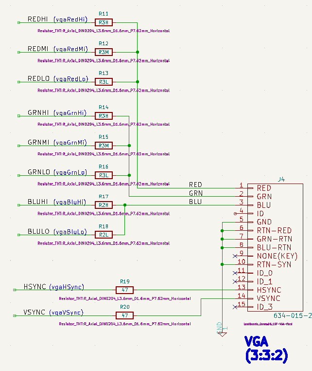
J4 - 3:3:2 VGA (256 colors
- VGA connector
- 8-bit video (3:3:2)
J5 - SD Card socket
J6, U1 - XIAO RP2040
- XIAO RP2040
- Can power the card from the USB on this card
- All pins are bought out to J1, J2 headers
- Used as an FTDI card replacement
- Tx/Rx/RTS/CTS brought to FPGA card
- Connected to SD Card
- SD Card is shared with FPGA
- Can be used as replacement disk drive for BASIC Load/Save commands
J7, J8 - FPGA Adapter Card
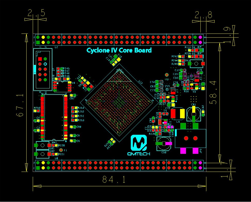
- QMTECH FPGA cards
- EP4CE15 Cyclone IV FPGA Card (tested)
- EP4CE55 Cyclone IV FPGA Card (untested)
- Cyclone V FPGA Card] (tested)
- Cyclone V FPGA Card (untested)
- QMTECH Cyclone 10CL006 FPGA Card (tested)
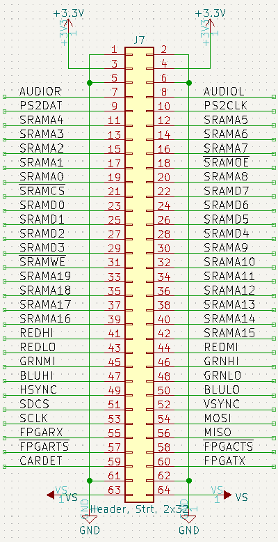
J7 - CPU I/O pins
- Connects to SRAM, PS/2, VGA, SD card
J7 Pins list
| U7 PIN | EP4CE15/55 | 5CEFA2 | CYC 10 | FUNCTION | U7 PIN | EP4CE15/55 | 5CEFA2 | CYC 10 | FUNCTION | |
|---|---|---|---|---|---|---|---|---|---|---|
| 1 | GND | GND | GND | GND | 2 | GND | GND | GND | GND | |
| 3 | 3.3V | 3.3V | 3.3V | 3.3V | 4 | 3.3V | 3.3V | 3.3V | 3.3V | |
| 5 | GND | GND | GND | GND | 6 | GND | GND | GND | GND | |
| 7 | PIN_R1 | PIN_AA2 | PIN_G1 | AUDIOR | 8 | PIN_R2 | PIN_AA1 | PIN_G2 | AUDIOL | |
| 9 | PIN_P1 | PIN_Y3 | PIN_D1 | PS2DAT | 10 | PIN_P2 | PIN_W2 | PIN_C2 | PS2CLK | |
| 11 | PIN_N1 | PIN_U1 | PIN_B1 | SRAMA4 | 12 | PIN_N2 | PIN_U2 | PIN_F5 | SRAMA5 | |
| 13 | PIN_M1 | PIN_N1 | PIN_D3 | SRAMA3 | 14 | PIN_M2 | PIN_N2 | PIN_C3 | SRAMA6 | |
| 15 | PIN_J1 | PIN_L1 | PIN_B3 | SRAMA2 | 16 | PIN_J2 | PIN_L2 | PIN_A3 | SRAMA7 | |
| 17 | PIN_H1 | PIN_G1 | PIN_B4 | SRAMA1 | 18 | PIN_H2 | PIN_G2 | PIN_A4 | SRAM0E_N | |
| 19 | PIN_F1 | PIN_E2 | PIN_E5 | SRAMA0 | 20 | PIN_F2 | PIN_D3 | PIN_A2 | SRAMA8 | |
| 21 | PIN_E1 | PIN_C1 | PIN_D4 | SRAMCS_N | 22 | PIN_D2 | PIN_C2 | PIN_E6 | SRAMD7 | |
| 23 | PIN_C1 | PIN_G6 | PIN_C6 | SRAMD0 | 24 | PIN_C2 | PIN_H6 | PIN_D6 | SRAMD6 | |
| 25 | PIN_B1 | PIN_G8 | PIN_B5 | SRAMD1 | 26 | PIN_B2 | PIN_H8 | PIN_A5 | SRAMD5 | |
| 27 | PIN_B3 | PIN_F7 | PIN_B6 | SRAMD2 | 28 | PIN_A3 | PIN_E7 | PIN_A6 | SRAMD4 | |
| 29 | PIN_B4 | PIN_D6 | PIN_B7 | SRAMD3 | 30 | PIN_A4 | PIN_C6 | PIN_A7 | SRAMA9 | |
| 31 | PIN_C4 | PIN_E9 | PIN_D8 | SRAMWE_N | 32 | PIN_C3 | PIN_D9 | PIN_C8 | SRAMA10 | |
| 33 | PIN_B5 | PIN_B5 | PIN_D9 | SRAMA19 | 34 | PIN_A5 | PIN_A5 | PIN_C9 | SRAMA11 | |
| 35 | PIN_B6 | PIN_B6 | PIN_B8 | SRAMA18 | 36 | PIN_A6 | PIN_B7 | PIN_A8 | SRAMA12 | |
| 37 | PIN_B7 | PIN_A7 | PIN_B9 | SRAMA17 | 38 | PIN_A7 | PIN_A8 | PIN_A9 | SRAMA13 | |
| 39 | PIN_B8 | PIN_A9 | PIN_E9 | SRAMA16 | 40 | PIN_A8 | PIN_A10 | PIN_E8 | SRAMA14 | |
| 41 | PIN_B9 | PIN_B10 | PIN_E11 | REDHI | 42 | PIN_A9 | PIN_C9 | PIN_E10 | SRAMA15 | |
| 43 | PIN_B10 | PIN_G10 | PIN_A10 | REDLO | 44 | PIN_A10 | PIN_F10 | PIN_B10 | REDMID | |
| 45 | PIN_B13 | PIN_C11 | PIN_D12 | GRNMID | 46 | PIN_A13 | PIN_B11 | PIN_D11 | GRNHI | |
| 47 | PIN_B14 | PIN_B12 | PIN_B11 | BLUHI | 48 | PIN_A14 | PIN_A12 | PIN_A11 | GRNLO | |
| 49 | PIN_B15 | PIN_E12 | PIN_B12 | HSYNC | 50 | PIN_A15 | PIN_D12 | PIN_A12 | BLULO | |
| 51 | PIN_B16 | PIN_D13 | PIN_B13 | SDCS_N | 52 | PIN_A16 | PIN_C13 | PIN_A13 | VSYNC | |
| 53 | PIN_B17 | PIN_B13 | PIN_B14 | SD_SCK | 54 | PIN_A17 | PIN_A13 | PIN_A14 | SD_MOSI | |
| 55 | PIN_B18 | PIN_A15 | PIN_D14 | USBTX/FPGARX | 56 | PIN_A18 | PIN_A14 | PIN_C14 | SD_MISO | |
| 57 | PIN_B19 | PIN_B15 | PIN_B16 | USBCTS/FPGARTS | 58 | PIN_A19 | PIN_C15 | PIN_A15 | UBSRTS/FPGACTS | |
| 59 | PIN_B20 | PIN_C16 | PIN_C16 | CD_DET | 60 | PIN_A20 | PIN_B16 | PIN_C15 | USBRX/FPGATX | |
| 61 | GND | GND | GND | GND | 62 | GND | GND | GND | GND | |
| 63 | 5V | 5V | 5V | 5V | 64 | 5V | 5V | 5V | 5V |
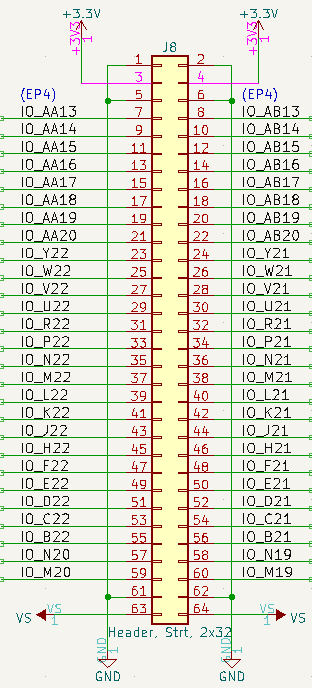
J8 - I/O pins (J8)
- All pins are usable and are daisy-chained to 3 expansion connectors
J8 Pins List
- Cyclone 10 FPGA notes
- Cannot place output or bidirectional pin J8IO[35] or pull-up in input pin location M16
- Cannot place output or bidirectional pin J8IO[36] or pull-up in input pin location M15
- Cannot place output or bidirectional pin J8IO[57] or pull-up in input pin location E16
- Cannot place output or bidirectional pin J8IO[58] or pull-up in input pin location E15
| U8 PIN | EP4CE15/55 | 5CEFA2 | 10C1006 | U8 PIN | EP4CE15/55 | 5CEFA2 | 10C1006 | |
|---|---|---|---|---|---|---|---|---|
| 1 | GND | GND | GND | 2 | GND | GND | GND | |
| 3 | 3.3V | 3.3V | 3.3V | 4 | 3.3V | 3.3V | 3.3V | |
| 5 | GND | GND | GND | 6 | GND | GND | GND | |
| 7 | PIN_AA13 | PIN_AA14 | PIN_R9 | 8 | PIN_AB13 | PIN_AA13 | PIN_T9 | |
| 9 | PIN_AA14 | PIN_AA15 | PIN_R10 | 10 | PIN_AB14 | PIN_AB15 | PIN_T10 | |
| 11 | PIN_AA15 | PIN_Y15 | PIN_R11 | 12 | PIN_AB15 | PIN_Y14 | PIN_T11 | |
| 13 | PIN_AA16 | PIN_AB18 | PIN_R12 | 14 | PIN_AB16 | PIN_AB17 | PIN_T12 | |
| 15 | PIN_AA17 | PIN_Y17 | PIN_N9 | 16 | PIN_AB17 | PIN_Y16 | PIN_M9 | |
| 17 | PIN_AA18 | PIN_AA18 | PIN_M10 | 18 | PIN_AB18 | PIN_AA17 | PIN_P9 | |
| 19 | PIN_AA19 | PIN_AA20 | PIN_P11 | 20 | PIN_AB19 | PIN_AA19 | PIN_N11 | |
| 21 | PIN_AA20 | PIN_Y20 | PIN_R13 | 22 | PIN_AB20 | PIN_Y19 | PIN_T13 | |
| 23 | PIN_Y22 | PIN_AB21 | PIN_T15 | 24 | PIN_Y21 | PIN_AB20 | PIN_T14 | |
| 25 | PIN_W22 | PIN_AA22 | PIN_N12 | 26 | PIN_W21 | PIN_AB22 | PIN_M11 | |
| 27 | PIN_V22 | PIN_W22 | PIN_R14 | 28 | PIN_V21 | PIN_Y22 | PIN_N13 | |
| 29 | PIN_U22 | PIN_Y21 | PIN_N14 | 30 | PIN_U21 | PIN_W21 | PIN_P14 | |
| 31 | PIN_R22 | PIN_U22 | PIN_P16 | 32 | PIN_R21 | PIN_V21 | PIN_R16 | |
| 33 | PIN_P22 | PIN_V20 | PIN_N16 | 34 | PIN_P21 | PIN_W19 | PIN_N15 | |
| 35 | PIN_N22 | PIN_U21 | PIN_M16 * | 36 | PIN_N21 | PIN_U20 | PIN_M15 * | |
| 37 | PIN_M22 | PIN_R22 | PIN_L16 | 38 | PIN_M21 | PIN_T22 | PIN_L15 | |
| 39 | PIN_L22 | PIN_P22 | PIN_P15 | 40 | PIN_L21 | PIN_R21 | PIN_M12 | |
| 41 | PIN_K22 | PIN_T20 | PIN_L14 | 42 | PIN_K21 | PIN_T19 | PIN_L13 | |
| 43 | PIN_J22 | PIN_P16 | PIN_K16 | 44 | PIN_J21 | PIN_P17 | PIN_K15 | |
| 45 | PIN_H22 | PIN_N20 | PIN_K12 | 46 | PIN_H21 | PIN_N21 | PIN_J12 | |
| 47 | PIN_F22 | PIN_M21 | PIN_J14 | 48 | PIN_F21 | PIN_M20 | PIN_J13 | |
| 49 | PIN_E22 | PIN_M18 | PIN_K11 | 50 | PIN_E21 | PIN_N19 | PIN_J11 | |
| 51 | PIN_D22 | PIN_L18 | PIN_G11 | 52 | PIN_D21 | PIN_L19 | PIN_F11 | |
| 53 | PIN_C22 | PIN_M22 | PIN_F13 | 54 | PIN_C21 | PIN_L22 | PIN_F14 | |
| 55 | PIN_B22 | PIN_L17 | PIN_F10 | 56 | PIN_B21 | PIN_K17 | PIN_F9 | |
| 57 | PIN_N20 | PIN_K22 | PIN_E16 * | 58 | PIN_N19 | PIN_K21 | PIN_E15 * | |
| 59 | PIN_M20 | PIN_M16 | PIN_D16 | 60 | PIN_M19 | PIN_N16 | PIN_D15 | |
| 61 | GND | GND | GND | 62 | GND | GND | GND | |
| 63 | 5V | 5V | 5V | 64 | 5V | 5V | 5V |
J10-J12 - 3 I/O slots IO_1-IO_3
- 3 I/O connectors
- 2x40 headers
- First 64-pins match pinout of J8
- Last 16 pins are chained together and do not connect to the FPGA (IOX65-80)
- Cyclone 10 notes
- Cannot place output or bidirectional pin J8IO[35] in input pin location M16
- Cannot place output or bidirectional pin J8IO[36] in input pin location M15
- Cannot place output or bidirectional pin J8IO[57] in input pin location E16
- Cannot place output or bidirectional pin J8IO[58] in input pin location E15
J10-J12 Pins List
| U8 PIN | EP4CE15/55 | 5CEFA2 | 10C1006 | U8 PIN | EP4CE15/55 | 5CEFA2 | 10C1006 | |
|---|---|---|---|---|---|---|---|---|
| 1 | GND | GND | GND | 2 | GND | GND | GND | |
| 3 | 3.3V | 3.3V | 3.3V | 4 | 3.3V | 3.3V | 3.3V | |
| 5 | GND | GND | GND | 6 | GND | GND | GND | |
| 7 | PIN_AA13 | PIN_AA14 | PIN_R9 | 8 | PIN_AB13 | PIN_AA13 | PIN_T9 | |
| 9 | PIN_AA14 | PIN_AA15 | PIN_R10 | 10 | PIN_AB14 | PIN_AB15 | PIN_T10 | |
| 11 | PIN_AA15 | PIN_Y15 | PIN_R11 | 12 | PIN_AB15 | PIN_Y14 | PIN_T11 | |
| 13 | PIN_AA16 | PIN_AB18 | PIN_R12 | 14 | PIN_AB16 | PIN_AB17 | PIN_T12 | |
| 15 | PIN_AA17 | PIN_Y17 | PIN_N9 | 16 | PIN_AB17 | PIN_Y16 | PIN_M9 | |
| 17 | PIN_AA18 | PIN_AA18 | PIN_M10 | 18 | PIN_AB18 | PIN_AA17 | PIN_P9 | |
| 19 | PIN_AA19 | PIN_AA20 | PIN_P11 | 20 | PIN_AB19 | PIN_AA19 | PIN_N11 | |
| 21 | PIN_AA20 | PIN_Y20 | PIN_R13 | 22 | PIN_AB20 | PIN_Y19 | PIN_T13 | |
| 23 | PIN_Y22 | PIN_AB21 | PIN_T15 | 24 | PIN_Y21 | PIN_AB20 | PIN_T14 | |
| 25 | PIN_W22 | PIN_AA22 | PIN_N12 | 26 | PIN_W21 | PIN_AB22 | PIN_M11 | |
| 27 | PIN_V22 | PIN_W22 | PIN_R14 | 28 | PIN_V21 | PIN_Y22 | PIN_N13 | |
| 29 | PIN_U22 | PIN_Y21 | PIN_N14 | 30 | PIN_U21 | PIN_W21 | PIN_P14 | |
| 31 | PIN_R22 | PIN_U22 | PIN_P16 | 32 | PIN_R21 | PIN_V21 | PIN_R16 | |
| 33 | PIN_P22 | PIN_V20 | PIN_N16 | 34 | PIN_P21 | PIN_W19 | PIN_N15 | |
| 35 | PIN_N22 | PIN_U21 | PIN_M16 | 36 | PIN_N21 | PIN_U20 | PIN_M15 | |
| 37 | PIN_M22 | PIN_R22 | PIN_L16 | 38 | PIN_M21 | PIN_T22 | PIN_L15 | |
| 39 | PIN_L22 | PIN_P22 | PIN_P15 | 40 | PIN_L21 | PIN_R21 | PIN_M12 | |
| 41 | PIN_K22 | PIN_T20 | PIN_L14 | 42 | PIN_K21 | PIN_T19 | PIN_L13 | |
| 43 | PIN_J22 | PIN_P16 | PIN_K16 | 44 | PIN_J21 | PIN_P17 | PIN_K15 | |
| 45 | PIN_H22 | PIN_N20 | PIN_K12 | 46 | PIN_H21 | PIN_N21 | PIN_J12 | |
| 47 | PIN_F22 | PIN_M21 | PIN_J14 | 48 | PIN_F21 | PIN_M20 | PIN_J13 | |
| 49 | PIN_E22 | PIN_M18 | PIN_K11 | 50 | PIN_E21 | PIN_N19 | PIN_J11 | |
| 51 | PIN_D22 | PIN_L18 | PIN_G11 | 52 | PIN_D21 | PIN_L19 | PIN_F11 | |
| 53 | PIN_C22 | PIN_M22 | PIN_F13 | 54 | PIN_C21 | PIN_L22 | PIN_F14 | |
| 55 | PIN_B22 | PIN_L17 | PIN_F10 | 56 | PIN_B21 | PIN_K17 | PIN_F9 | |
| 57 | PIN_N20 | PIN_K22 | PIN_E16 | 58 | PIN_N19 | PIN_K21 | PIN_E15 | |
| 59 | PIN_M20 | PIN_M16 | PIN_D16 | 60 | PIN_M19 | PIN_N16 | PIN_D15 | |
| 61 | GND | GND | GND | 62 | GND | GND | GND | |
| 63 | 5V | 5V | 5V | 64 | 5V | 5V | 5V | |
| 65 | IOX_65 | IOX_65 | IOX_65 | 66 | IOX_66 | IOX_66 | IOX_66 | |
| 67 | IOX_67 | IOX_67 | IOX_67 | 68 | IOX_68 | IOX_68 | IOX_68 | |
| 69 | IOX_69 | IOX_69 | IOX_69 | 70 | IOX_70 | IOX_70 | IOX_70 | |
| 71 | IOX_71 | IOX_71 | IOX_71 | 72 | IOX_72 | IOX_72 | IOX_72 | |
| 73 | IOX_73 | IOX_73 | IOX_73 | 74 | IOX_74 | IOX_74 | IOX_74 | |
| 75 | IOX_75 | IOX_75 | IOX_75 | 76 | IOX_76 | IOX_76 | IOX_76 | |
| 77 | IOX_77 | IOX_77 | IOX_77 | 78 | IOX_78 | IOX_78 | IOX_78 | |
| 79 | IOX_79 | IOX_79 | IOX_79 | 80 | IOX_80 | IOX_80 | IOX_80 | |
| IOX_81 | IOX_81 | IOX_81 | 82 | IOX_82 | IOX_82 | IOX_82 |
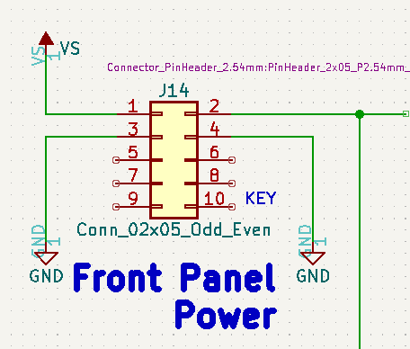
J14 - Power LEDs
J15 - Reset Switch
- Right angle header
- Connects to J8-35
- Attach case reset line here
- Cyclone 10 does not have internal weak pull up for this pin
J16 - Power Switch
- Connects to case power switch
- Shuts off power from USB B
- Does not affect power from RP2040 card
H1 - I/O Slots Power Select Jumper
- Can use 3.3V from FPGA card or on-board 3.3V regulator
170x170mm, Mini-ITX card
- Thin Mini-ITX Based PC System Design Guide - Intel
- MINI ITX SPEC V2 0
- Mini-ITX Interface Specification, version 1.1/1.2
- Thin Mini-ITX Based All-In-One PC Compliance Requirements
- 4mm Mounting holes for Mini ITX case
- Isolated pads
- M06 Mini Desktop Case J8G3
- TX02 Mini Desktop Case J6E2
- MATX ATX PC Test Bench Open Air Frame Overclock Case
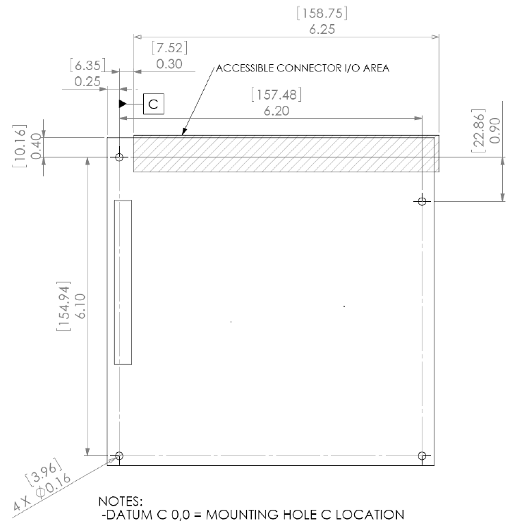
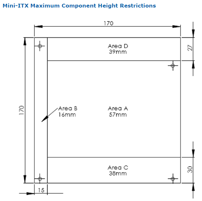
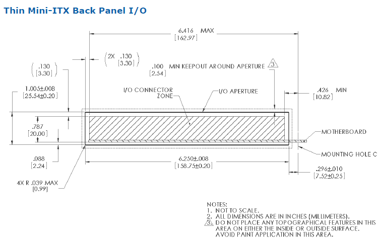
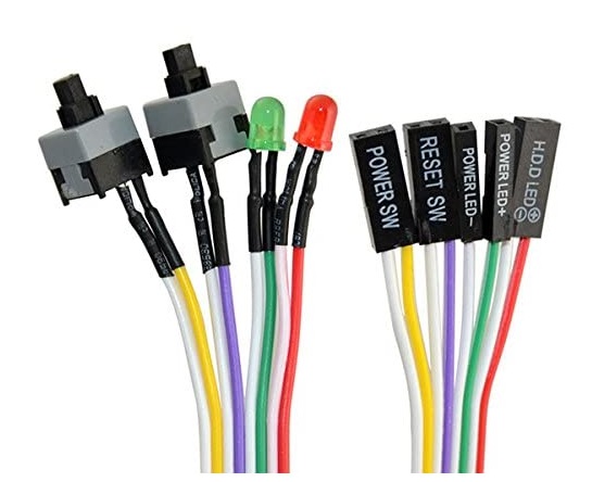
Card Mechanicals
Card Height
Back Panel
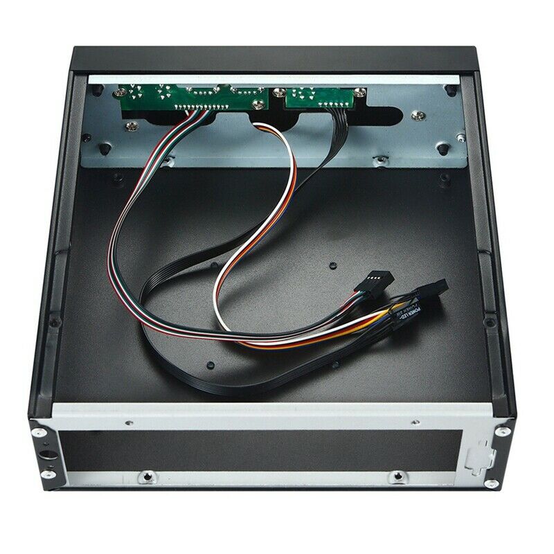
Case Cabling
Expansion Cards
FPGA-ITX-01 expansion cards plug into the expansion connectors to expand the functionality of the FPGA design.
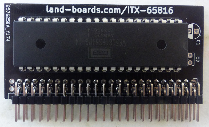
ITX-65C816
- ITX-65C816
- W65C816 CPU module
- 3.3V
- Running at 8.33 MHz
- Native mode (65C816 extended code) and emulation mode (65C02 code)
- Native mode allows for 24-bit address space
ITX-PI-PICO
- ITX-PI-PICO
- Raspberry Pi Pico Module
ITX-BKOUT
- ITX-BKOUT
- Breakout card which connects to the pins of the expansion connectors with power/ground down the center of the card.
- Configured as Bus Monitor for Logic Analyzer
ITX-SWLEDs
- ITX-SWLEDs
- 8 pushbuttons, 8 slide switches, 16 LEDs.
Mechanicals
- QMTECH FPGA card
Software
Software that runs on the card
Multicomp Builds
Tested Multicomp builds
- M6502_VGA_Int65C816_Cyclone10
- M6800_MIKBUG
- M6809_VGA_PS2_RAM(56K)
- MultiComp_6809_by_Neal_C-2019-04-08
- Multicomp-MPM
- UK101_41K
XIAO RP2040
- USB-SERIAL - Arduino sketch turns the RP2040 into a USB to Serial Bridge
- Runs at 115,200 baud
- Hardware Handshake implemented
- Only uses RTS output from the FPGA to hold off output
- Most Multicomp builds switch I/O with F1 key
- TeraTerm at 115,200 baud
Revision History
Rev 2
- Moved upper right mounting hole
- Fixed R23 DRC
- Add pull-up resistors for input only pins
- J8-35, 36, 57, 58
- Move silkscreen pin numbers around FPGA a bit
- Widen JTAG silkscreen block
- Verified pin No Connects are correct
- Added Rev 2 marking
- Change R2H, etc to call out R/G/B (match PL)
Rev 1
- Upper right mounting hole (near XAIO USB/Serial interface) is in wrong spot
- At 0.9" from edge, should be 0.9" from upper left mounting hole
- Not big issue, no mechanical interference on board, just use 3 mounting holes to install in case
- Yabs = 2.47480315, change to 2.87480315
- R23 DRC error
- Overshot pin on rear side
- Verified right pin is connected
- Input only pins (using Cyclone 10) do not support internal pull-ups
- Missing Rev marking (use P-Touch label)
- Tested/works
- Video
- PS/2 keyboard
- SD card
- 5V input
