Difference between revisions of "DiffProbe"
Jump to navigation
Jump to search
Blwikiadmin (talk | contribs) |
Blwikiadmin (talk | contribs) |
||
| (25 intermediate revisions by the same user not shown) | |||
| Line 1: | Line 1: | ||
| + | [[File:tindie-mediums.png|link=https://www.tindie.com/products/land_boards/differential-scope-probe-pcb-only/]] | ||
| + | |||
== Differential Oscilloscope Probe == | == Differential Oscilloscope Probe == | ||
| Line 12: | Line 14: | ||
<video type="youtube">cWtCm04bhXQ</video> | <video type="youtube">cWtCm04bhXQ</video> | ||
| + | |||
| + | === Other Video === | ||
| + | |||
| + | <video type="youtube">RDLWQFgJ1uU</video> | ||
| + | |||
| + | <video type="youtube">OZDijMDHmtI</video> | ||
=== Linear Tech Design === | === Linear Tech Design === | ||
| Line 19: | Line 27: | ||
[[File:LTC6268-10_isoSPI_DiffAmp.png]] | [[File:LTC6268-10_isoSPI_DiffAmp.png]] | ||
| − | ( | + | (PCB Image is from Linear Tech website) |
== Features == | == Features == | ||
* This circuit uses two LT6268 high-frequency amplifiers to realize a fully differential oscilloscope probe | * This circuit uses two LT6268 high-frequency amplifiers to realize a fully differential oscilloscope probe | ||
| − | * >100MHz bandwidth | + | * >100MHz bandwidth (dependent on op amp part speed grade selected) |
| − | * 100kilohm input resistance on 1:1 allowing signals up to +/- 2.5V | + | * Build options (R1/R3, R2/R5 ratios values) |
| − | * 1Megohm input resistance on 10:1 allowing signals up to +/- 25V | + | ** 100kilohm input resistance on 1:1 allowing signals up to +/- 2.5V |
| + | ** 1Megohm input resistance on 10:1 allowing signals up to +/- 25V | ||
* The input stage is a modified differential amplifier configuration with 100:1 attenuation on the inputs to allow wide common-mode swings | * The input stage is a modified differential amplifier configuration with 100:1 attenuation on the inputs to allow wide common-mode swings | ||
* The inputs are ac-coupled to provide high-voltage dc blocking | * The inputs are ac-coupled to provide high-voltage dc blocking | ||
| Line 32: | Line 41: | ||
* A back-termination resistor provides stability when driving a cable to the 1Megohm oscilloscope input port, and is AC-coupled to remove the 2.5V output-stage bias | * A back-termination resistor provides stability when driving a cable to the 1Megohm oscilloscope input port, and is AC-coupled to remove the 2.5V output-stage bias | ||
* The circuit is powered from 5V, derived from a 9V battery with an LDO | * The circuit is powered from 5V, derived from a 9V battery with an LDO | ||
| + | * 16.5mA per amplifier | ||
* Power Switch for battery operation | * Power Switch for battery operation | ||
* Power Indicator LED | * Power Indicator LED | ||
| Line 39: | Line 49: | ||
* Due to the wide bandwidth amplifiers and the relatively high resistances being used, stray capacitance control and careful layout is vital | * Due to the wide bandwidth amplifiers and the relatively high resistances being used, stray capacitance control and careful layout is vital | ||
* A 'gimmick' feedback capacitor may be needed to adjust the damping of the amplifiers to avoid oscillation and to achieve best time-response | * A 'gimmick' feedback capacitor may be needed to adjust the damping of the amplifiers to avoid oscillation and to achieve best time-response | ||
| − | * | + | * Can scale the input voltage by selecting different input resistor values |
| + | |||
| + | ==== Gimmick Cap ==== | ||
| + | |||
| + | [[File:GimmickCap.PNG]] | ||
=== Other Ap Notes === | === Other Ap Notes === | ||
| Line 61: | Line 75: | ||
* [http://www.linear.com/solutions/6058 LTSpice Model] | * [http://www.linear.com/solutions/6058 LTSpice Model] | ||
| − | == | + | == Schematic == |
| + | |||
| + | [http://land-boards.com/DIFFPROBE/DiffProbe-Schematic-RevX2.pdf Rev X2 Schematic] | ||
| + | |||
| + | == Input Cabling == | ||
| + | |||
| + | [[File:DiffProbeCabled-720px-P585.jpg]] | ||
| + | |||
| + | [[File:DiffProbeCabled-720px-P586.jpg]] | ||
| − | [[File:DiffProbe- | + | == Why? - Isolation from earth == |
| + | |||
| + | [[File:ds1054z-grounds.jpg]] | ||
| + | |||
| + | == Board Layout - Rev X2 == | ||
| + | |||
| + | [[File:DiffProbe-BothSides-X2bw.png]] | ||
| + | |||
| + | == Rev X1 == | ||
[[File:DiffProbe-Rear-720px-P583.jpg]] | [[File:DiffProbe-Rear-720px-P583.jpg]] | ||
| + | |||
| + | == Expensive Commercial Unit == | ||
| + | |||
| + | [[File:DiffProbe.PNG]] | ||
== Connectors == | == Connectors == | ||
| Line 80: | Line 114: | ||
* Female BNC connector | * Female BNC connector | ||
| − | + | ** Use male-male coupler or BNC-to-BNC cable to connect to scope | |
=== J3 - Input === | === J3 - Input === | ||
| Line 88: | Line 122: | ||
# + (Plus side of differential probe) | # + (Plus side of differential probe) | ||
# - (Minus side of differential probe) | # - (Minus side of differential probe) | ||
| + | |||
| + | === J4 - Power (alternate to J1) === | ||
| + | |||
| + | * 2 pin, 0.1" pitch | ||
== Assembly Sheet == | == Assembly Sheet == | ||
[[Differential Probe Assembly Sheet]] | [[Differential Probe Assembly Sheet]] | ||
Latest revision as of 14:03, 6 July 2023
Contents
Differential Oscilloscope Probe
Videos
Other Video
Linear Tech Design
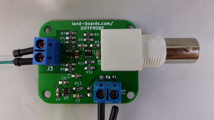
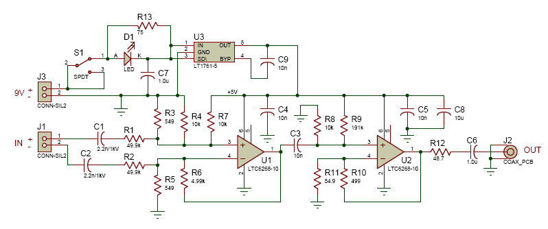
This differential oscilloscope probe is based on a Linear Technology application note. The design uses LTC6268-10 op amps which are 4GHz FET input operational amplifiers with extremely low input bias current and low input capacitance.
(PCB Image is from Linear Tech website)
Features
- This circuit uses two LT6268 high-frequency amplifiers to realize a fully differential oscilloscope probe
- >100MHz bandwidth (dependent on op amp part speed grade selected)
- Build options (R1/R3, R2/R5 ratios values)
- 100kilohm input resistance on 1:1 allowing signals up to +/- 2.5V
- 1Megohm input resistance on 10:1 allowing signals up to +/- 25V
- The input stage is a modified differential amplifier configuration with 100:1 attenuation on the inputs to allow wide common-mode swings
- The inputs are ac-coupled to provide high-voltage dc blocking
- The first-stage IC re-amplifies the signal by 10:1 as does the single-ended output stage, for a composite gain of 1:1
- A back-termination resistor provides stability when driving a cable to the 1Megohm oscilloscope input port, and is AC-coupled to remove the 2.5V output-stage bias
- The circuit is powered from 5V, derived from a 9V battery with an LDO
- 16.5mA per amplifier
- Power Switch for battery operation
- Power Indicator LED
Additional Design Notes
- Due to the wide bandwidth amplifiers and the relatively high resistances being used, stray capacitance control and careful layout is vital
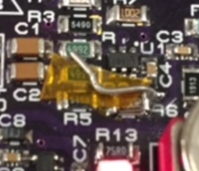
- A 'gimmick' feedback capacitor may be needed to adjust the damping of the amplifiers to avoid oscillation and to achieve best time-response
- Can scale the input voltage by selecting different input resistor values
Gimmick Cap
Other Ap Notes
- Gimmick Capacitor Stabilizes High-Frequency Op Amps
- RG58C Coaxial Cable, BNC Male / Male, 1.5 ft]
- 50cm RG58 Cable BNC Male Plug To BNC Male Straight Crimp Coax Pigtail 20in
- Why Op Amps Oscillate—an intuitive look at two frequent causes
- SPICEing Op Amp Stability
- PSPICE Performs Op Amp Open Loop Stability Analysis (HA5112)
- Solving Op Amp Stability Issues
Linear Tech Application Note
(Image from the Linear Tech website)
Schematic
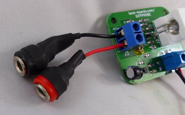
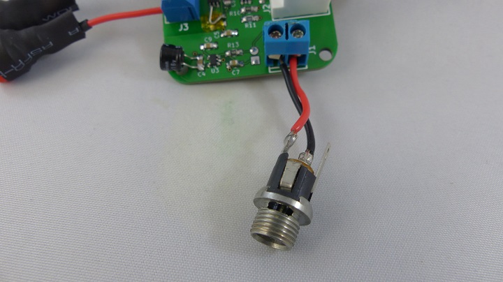
Input Cabling
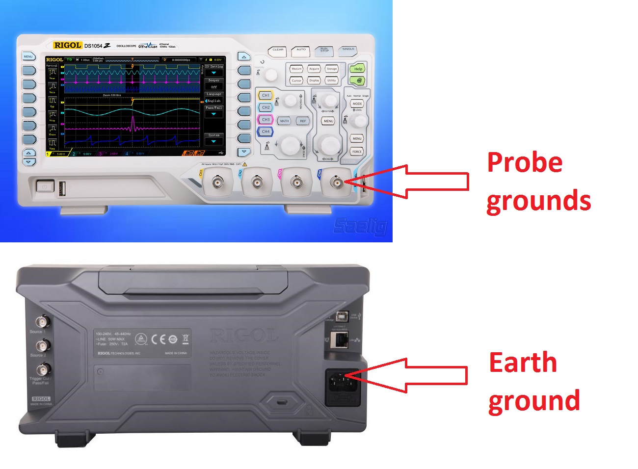
Why? - Isolation from earth
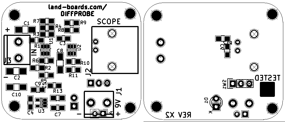
Board Layout - Rev X2
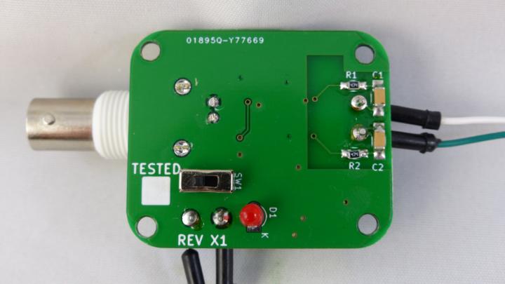
Rev X1
Expensive Commercial Unit
Connectors
J1 - Power
- 6-9V DC Input power
- 2-pin, 5mm pitch terminal block connector
- Pinout
- +VCC
- GND
J2 BNC Output (to Scope)
- Female BNC connector
- Use male-male coupler or BNC-to-BNC cable to connect to scope
J3 - Input
- 2-pin, 5mm pitch terminal block connector
- Pinout
- + (Plus side of differential probe)
- - (Minus side of differential probe)
J4 - Power (alternate to J1)
- 2 pin, 0.1" pitch

