Difference between revisions of "OPTOFAST"
Jump to navigation
Jump to search
Blwikiadmin (talk | contribs) |
Blwikiadmin (talk | contribs) |
||
| Line 1: | Line 1: | ||
[[File:tindie-mediums.png|link=https://www.tindie.com/products/land_boards/4-channel-opto-coupler-card-optofast/]] | [[File:tindie-mediums.png|link=https://www.tindie.com/products/land_boards/4-channel-opto-coupler-card-optofast/]] | ||
| + | |||
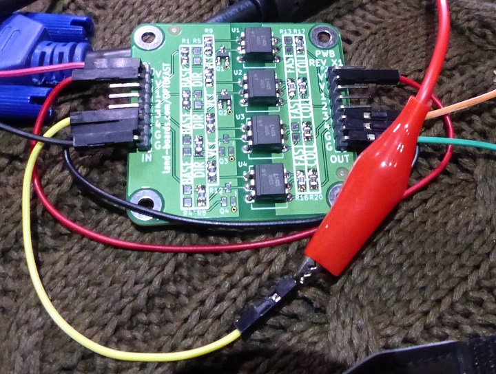
| + | [[file:2017-01-28T19_42_37.589Z-OPTOFAST-P668-720px.jpg]] | ||
== OPTOFAST - 4 Channel Optocoupler Card == | == OPTOFAST - 4 Channel Optocoupler Card == | ||
Revision as of 21:43, 13 March 2022
File:2017-01-28T19 42 37.589Z-OPTOFAST-P668-720px.jpg
Contents
OPTOFAST - 4 Channel Optocoupler Card
See our other Optocoupler cards
- OPTOFAST-2 - Speed improved 4 channel optocoupler card - Suggested replacement for this card
- OPTOSMALL - Four channel optocoupler card
- OPTOOUT8-I2C - Eight channel optocoupler card - I2C interface
- OPTOUSB - Optically coupled USB to FTDI interface
- OPTOFASTBI - Two Optos in Two Directions
Features
- Opto-Isolator card
- 4-Channels
- 4N25 Optoisolators
- Input /Output isolation
- Transistor driver for Opto LED reduces required drive from 10 mA to under 500 uA
- Input channels share their own common VCC/Ground
- Output channels share their own common Vcc/Ground
- 8-pin header for input
- 8-pin header for output
- Configuration Options (Speed enhanced, Bypass Input transistors, Remove Output collector resistors)
- 49x49mm
- (4) 4-40 mounting holes
Schematic (One channel)
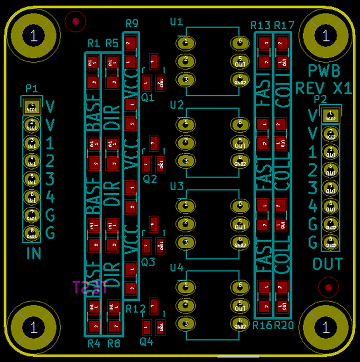
- U1 represents U1-U4 (channels 1-4)
- Q1 represents Q1-Q4 (channels 1-4)
- R1 (VCC) represents R1,R4,R7,R10 (channels 1-4)
- R2 (DIR) represents R2,R5,R8,R11 (channels 1-4)
- R3 (BASE) represents R3,R6,R8,R12 (channels 1-4)
- R13 (FAST) represents R13-R16 (channels 1-4)
- R17 (COLL) represents R17-R20 (channels 1-4)
Input Options
- Refer to schematic for impact of options
Use Input Transistor - Standard Option
- Common VCC in option
- Install transistor Q1
- R1 = 150
- LED current is 3.5V/150 Ohms = 23 mA
- CTR = .20, 4.7 mA
- R2 = Do not populate
- R3 = 10K
- Base drive ~ (Vin - 0.7V)/R3
- At 5V drive this is 4.3V/R3
- Using R3=10K at 5V this is 0.43mA Ib
- HFE (MMBT3904) = 100 min
- That is potentially 43 mA (in the switching range of the transistor)
- Collector resistor and LED voltage drop are current limiter
- At 3.3V drive this is (3.3-0.7)/10K = .26mA Ib
- HFE = 100 min
- That is 26 mA (in the switching range of the transistor)
- H1 do not short
Direct Drive - Special Option
- Do not install Q1
- Do not install R1
- R2 = 150
- Input current = LED current = 3.5V/150 Ohms = 23 mA
- Do not install R3
- Do not install Q1
- Short H1
Output Options
Standard Output
- R17 = 1.2K
- 5V/1.2K = 4.1mA of output transistor B-E current
- Leaves 4.7-4.1 mA = 600 uA of output low current
Open Collector Output - Special Option
- Do not install R17
Fast Option - Standard
- R13 = 20K (empirically determined from the scope eye)
Connectors
P1 - Input
8-pin, right angle, 0.1" pitch
- Vcc (In)
- Vcc (In)
- IN 1
- IN 2
- IN 3
- IN 4
- GND (In)
- GND (In)
P2 - Output
8-pin, right angle, 0.1" pitch
- Vcc (Out)
- Vcc (Out)
- OUT 1
- OUT 2
- OUT 3
- OUT 4
- GND (Out)
- GND (Out)
Test Card Measurements
Setup
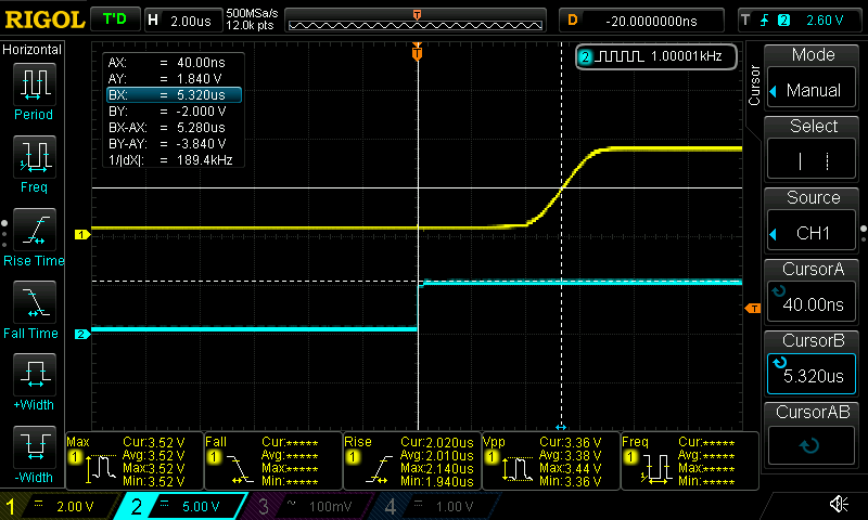
- Goal was to determine the performance of the OPTOFAST card
- 5V operation
- Same 5V input/output power supply
- Each of the channels were configured uniquely/individually
- MHS-5200A - Digital DDS Dual-channel Signal Generator
- 1 KHz square wave
- 5V signal level
- Single channel checked at a time
- Oscilloscope
- Rigol DS1054Z
- 50 MHz
- Ultra Sigma software used for screen captures
Notes
- Note that the input buffer transistor inverts the signal
- Built a card that has four different configurations
- Options
- Fast/Slow
- Direct drive input LED/Transistor Buffered input
Test Results
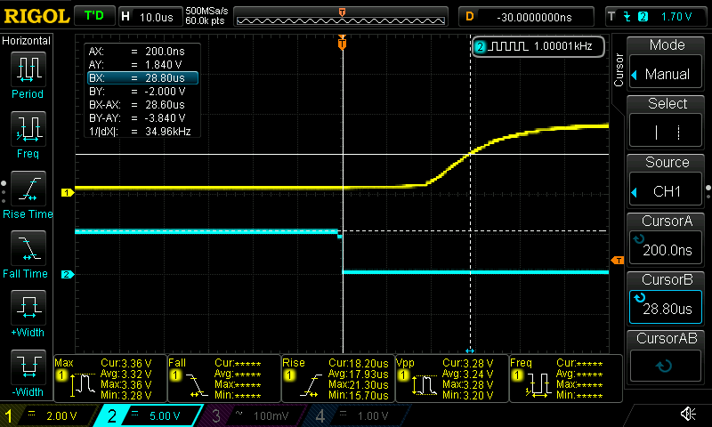
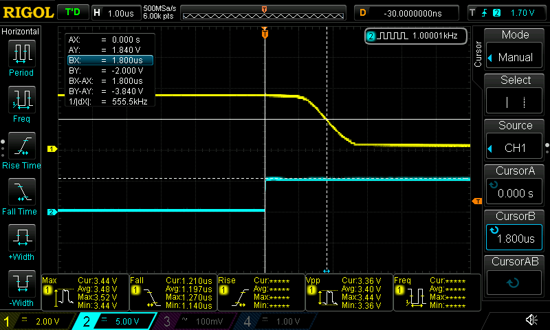
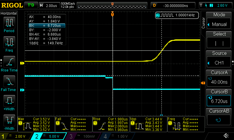
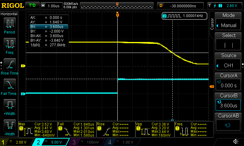
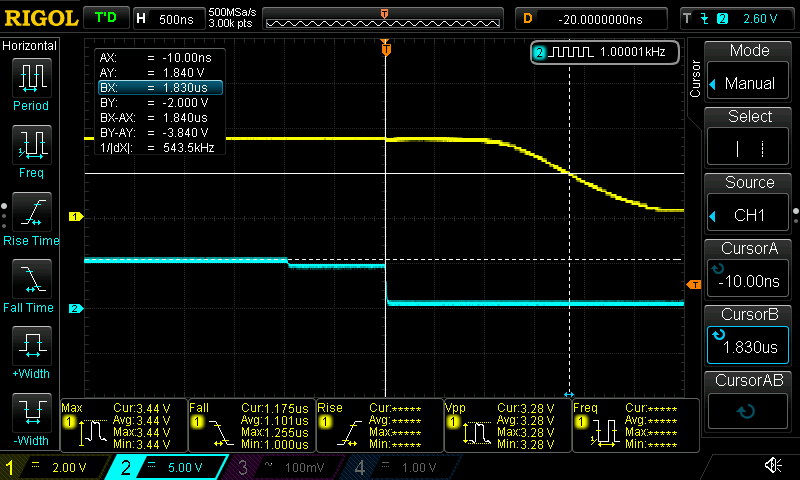
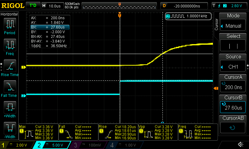
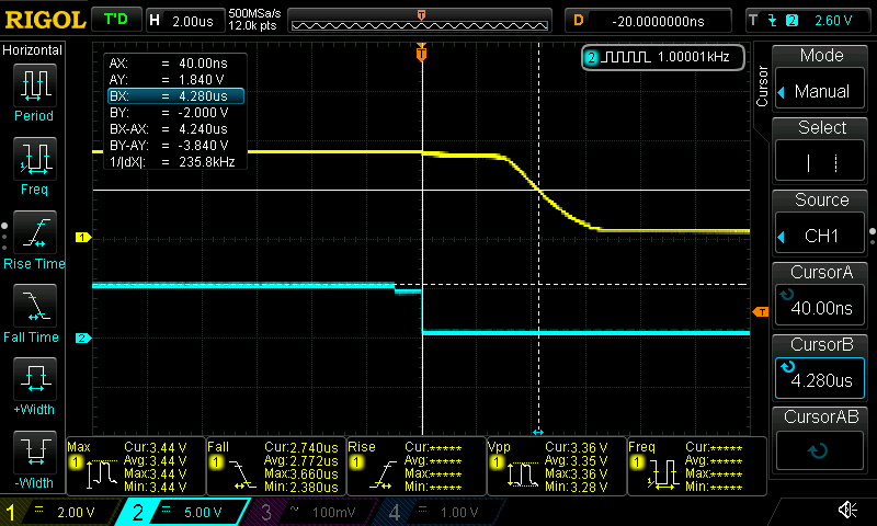
- Channel Fast/Slow TransBuff/Direct Input Rise/Fall Time(uS)
1 Slow Transistor Buffer Fall 28.6 1 Slow Transistor Buffer Rise 1.8 2 Fast Transistor Buffer Fall 6.68 2 Fast Transistor Buffer Rise 3.6 3 Slow Direct Input Fall 1.84 3 Slow Direct Input Rise 27.4 4 Fast Direct Input Fall 4.24 4 Fast Direct Input Rise 5.28


