Difference between revisions of "ODAS-PSOC5"
Jump to navigation
Jump to search
Blwikiadmin (talk | contribs) |
Blwikiadmin (talk | contribs) |
||
| Line 237: | Line 237: | ||
* [[Arduino Based Test Station]] | * [[Arduino Based Test Station]] | ||
** [[LED-32]] | ** [[LED-32]] | ||
| − | * Bounce a bit across the LEDs | + | * (2) [[LED-TEST-2]] cards |
| + | ** Bounce a bit across the LEDs | ||
[[file:ODAS-PSOC5_P1179_720px.jpg]] | [[file:ODAS-PSOC5_P1179_720px.jpg]] | ||
[[file:LED-TEST-2_TEST-P676-720px.jpg]] | [[file:LED-TEST-2_TEST-P676-720px.jpg]] | ||
| − | |||
| − | |||
== Software == | == Software == | ||
* [https://github.com/land-boards/ODAS/tree/master/ODAS-PSOC5/Projects GitHub Repository] | * [https://github.com/land-boards/ODAS/tree/master/ODAS-PSOC5/Projects GitHub Repository] | ||
Revision as of 14:40, 15 March 2022
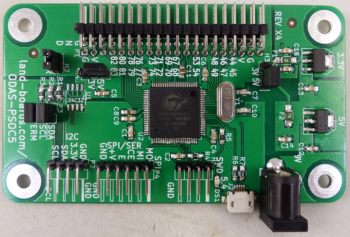
Features
- PSOC part CY8C5267AXI-LP051
- Core: ARM Cortex M3
- Data Bus Width: 32 bit
- Maximum Clock Frequency: 67 MHz
- Program Memory Size: 128 kB
- Data RAM Size: 32 kB
- ADC Resolution: 12 bit
- Data RAM Type: SRAM
- Interface Type: I2C, USB
- Number of ADC Channels: 1
- Number of I/Os: 72 I/O
- Number of Timers/Counters: 4 Timers
- Program Memory Type: Flash
- 16 MHz External Crystal
- Connectors
- USB Connector (USB-B Mini)
- I/O Connector (30 I/O lines which can be analog or digital connections)
- I2C Connector (4-pin header)
- SPI Connector (6-pin header)
- Configuration EEPROM
- 9V power input
- Fuses on 3.3V and 5V power
- 95x45mm Form Factor
- Compatible with Land Boards Open Data Acquisition System (ODAS) Cards
- (4) #6 screw holes for solid mounting
Headers
H1 - PSOC Programming Header
- SWDIO
- SWDCLK
- RESET
- GND
H2 - EEPROM Write Enable
- Install to enable EEPROM writes
H3 - I/O Voltage Zone 3 (VZ3)
- 1-2 = 3.3V
- 2-3 = 5V
- Connects to J1 VZ3 pins
H4 - I/O Voltage Zone 0 (VZ0)
- 1-2 = 3.3V
- 2-3 = 5V
- Connects to J1 VZ0 pins
Connectors
J1 - Power
- 7-12V in
- Regulator provides 5V to card
- Fuse protected 5V and 3.3V power distribution
J2 - USB Micro B
- Power not connected through this connector
P1
| Pin | Descr | Pin | Descr | |
|---|---|---|---|---|
| 1 | GND | 2 | GND | |
| 3 | VCC (Zone 0) | 4 | VCC (Zone 0) | |
| 5 | Pin.85 | 6 | Pin.84 | |
| 7 | Pin.83 | 8 | Pin.82 | |
| 9 | Pin.81 | 10 | Pin.80 | |
| 11 | Pin.79 | 12 | Pin.78 | |
| 13 | Pin.77 | 14 | Pin.76 | |
| 15 | Pin.74 | 16 | Pin.73 | |
| 17 | Pin.72 | 18 | Pin.71 | |
| 19 | Pin.70 | 20 | Pin.69 | |
| 21 | Pin.68 | 22 | Pin.67 | |
| 23 | Pin.56 | 24 | Pin.55 | |
| 25 | Pin.54 | 26 | Pin.53 | |
| 27 | Pin.52 | 28 | Pin.51 | |
| 29 | Pin.49 | 30 | Pin.48 | |
| 31 | Pin.47 | 32 | Pin.46 | |
| 33 | Pin.45 | 34 | Pin.44 | |
| 35 | VCC (Zone 3) | 36 | VCC (Zone 3) | |
| 37 | GND | 38 | GND | |
| 39 | N/C | 40 | N/C |
P2 - I2C Master (or Slave)
- GND
- 3.3V
- SDA
- SCL
P3 - I2C Terminator
- Install headers to enable terminators
- 1-2 SDA 3.3K Terminator
- 3-4 SCL 3.3K Terminator
P4 - SPI
- SPI_MOSI
- SPI_MISO
- SPI_CK
- SPI_CE0
- +3.3V
- GND
Programming
- Program using PSOC Creator
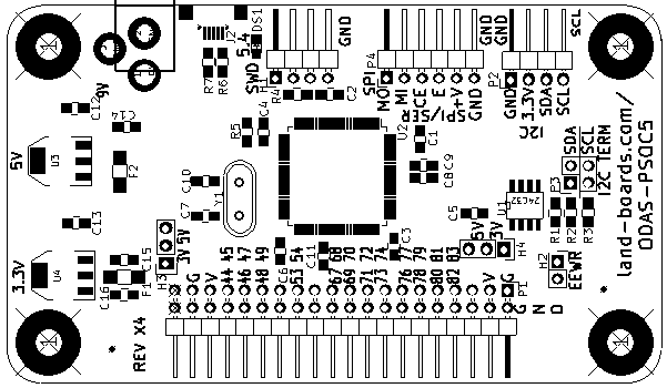
CAD - Rev X4
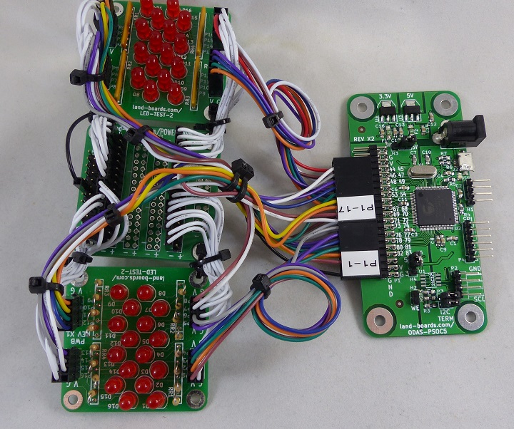
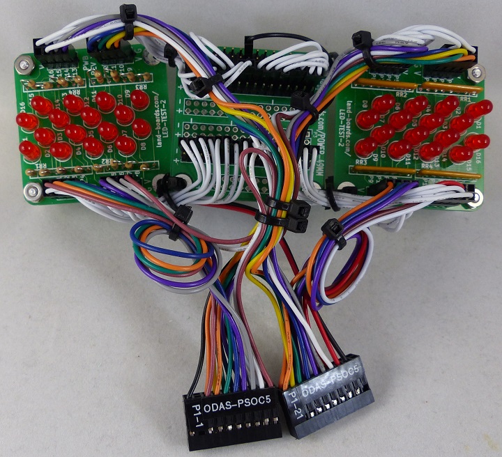
Test Setup
- Arduino Based Test Station
- (2) LED-TEST-2 cards
- Bounce a bit across the LEDs


