Difference between revisions of "IOP16 ANSI Display"
Jump to navigation
Jump to search
Blwikiadmin (talk | contribs) |
Blwikiadmin (talk | contribs) |
||
| Line 54: | Line 54: | ||
<pre> | <pre> | ||
| − | RTS | + | WRVDU JSR WTVDUTXRDY WAIT VDU TX READY |
| − | + | IOW 0X01 0X0B WRITE OUT R1 TO SCREEN | |
| − | + | RTS | |
| − | + | WTVDUTXRDY IOR 0X00 0X0A READ VDU STATUS | |
| − | + | ARI 0X00 0X02 TX EMPTY FLAG | |
| − | + | BEZ WTVDUTXRDY WAIT UNTIL TX EMPTY | |
| + | RTS | ||
</pre> | </pre> | ||
Revision as of 16:20, 16 April 2022
Contents
Multicomp FPGA (VHDL Template) VGA
Interface mimics ACIA software interface address/control/status contents
Programming Interface
- Two addresses, Control/status and data access
Status Register
- Register Select = 0
- Read/Write = Read
- d0 = RDRF = Receive Data Register Full (1 = data is ready to read)
- d1 = TDRE = Transmit Data Register Empty (1 = transmit is ready to send out data)
- d2 = DCD = Data Carrier Detect (0 = carrier present - hardwired)
- d3 = CTS = Clear to Send (0 = Clear to Send - ready to accept data - hardwired)
- d7 = IRQ = Interrupt Request (1 = Interrupt present)
Control Register
- Register Select = 0
- Read/Write = Write
- d1,d0 = Control (11 = Master Reset)
- d6,d5 = TC = Transmitter Control (RTS = Transmitter Interrupt Enable/Disable)
- d7 = Interrupt Enable (1=enable interrupts)
Data Register
- Register Select = 1
- Read = Read data from the data register (not implemented due to kbd removal)
- Write = Write data to the data register
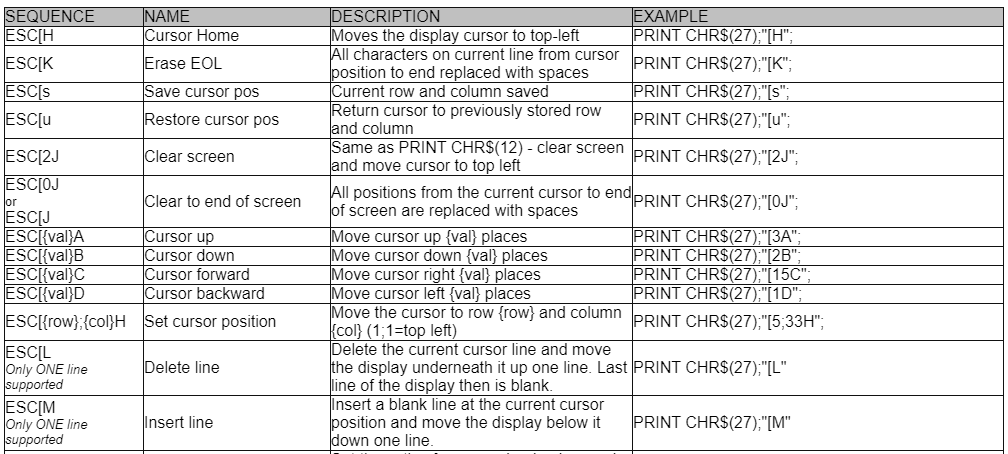
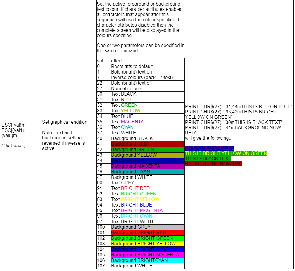
ANSI ESC Codes
ANSI Display Subroutines
- Initialize the VDU
INITVDU	LRI	0X00	0X03	RESET TERMINAL COMMAND
	IOW	0X00	0X0A	WRITE VDU CMD REG
	LRI	0X00	0X20	TX CTRLS RTS
	IOW	0X00	0X0A	WRITE VDU CMD REG
	RTS
- Write to the VDU
WRVDU		JSR	WTVDUTXRDY		WAIT VDU TX READY
		IOW	0X01		0X0B	WRITE OUT R1 TO SCREEN
		RTS
WTVDUTXRDY	IOR	0X00	0X0A		READ VDU STATUS
		ARI	0X00	0X02		TX EMPTY FLAG
		BEZ	WTVDUTXRDY		WAIT UNTIL TX EMPTY
		RTS
VHDL Code
Entity
-- ____________________________________________________________________________________
-- Grant Searle's VGA driver from Multicomp
-- DGG removed the PS/2 keyboard, Composite output and CTS
-- Interface matches ACIA software interface address/control/status contents

vdu : entity work.ANSIDisplayVGA
  GENERIC map (
    EXTENDED_CHARSET    => 0, -- 1 = 256 chars
                              -- 0 = 128 chars
    COLOUR_ATTS_ENABLED => 0, -- 1 = Color for each character
                              -- 0 = Color applied to whole display
    SANS_SERIF_FONT     => 1  -- 0 => use conventional CGA font
                              -- 1 => use san serif font
)
  port map (
    clk     => i_clk,
    n_reset => w_resetClean_n,
    -- CPU interface
    n_WR    => not W_VDUWr,
    n_rd    => not W_VDURd,
    regSel  => w_periphAdr(0),
    dataIn  => w_periphOut,
    dataOut => w_VDUDataOut,
    -- VGA video signals
    hSync   => hSync,
    vSync   => vSync,
    videoR0 => videoR0,
    videoR1 => videoR1,
    videoG0 => videoG0,
    videoG1 => videoG1,
    videoB0 => videoB0,
    videoB1 => videoB1
);
Signals
-- Decodes/Strobes
...
  signal W_VDUWr       : std_logic;
  signal W_VDURd       : std_logic;

-- Interfaces
...
  signal w_VDUDataOut  :  std_logic_vector(7 downto 0);
Hook-up code
-- Strobes/Selects
...
w_VDUWr <= '1' when ((w_periphAdr(7 downto 1) = "0000101") and (w_periphWr= '1')) else '0';
w_VDURd <= '1' when ((w_periphAdr(7 downto 1) = "0000101") and (w_periphRd = '1')) else '0';

-- Peripheral bus read mux
w_periphIn <=	...
  w_VDUDataOut			when w_periphAdr(7 downto 1) = "0000101"	else
...
Resources (10CL006)
- Logic Cells: 918
- Registers: 203
- Memory Bits: 24576 (128 chars)
- M9Ks: 3 (128 chars)
- Memory Bits: 32768 (256 chars)
- M9Ks: 4 (256 chars)
- Resource usage can be reduced by changing the generics below
- EXTENDED_CHARSET=0, COLOUR_ATTS_ENABLED=0 - Uses 3 M9K blocks
- EXTENDED_CHARSET=1, COLOUR_ATTS_ENABLED=0 - Uses 4 M9K blocks
- EXTENDED_CHARSET=0, COLOUR_ATTS_ENABLED=1 - Uses 5 M9K blocks
- EXTENDED_CHARSET=1, COLOUR_ATTS_ENABLED=1 - Uses 6 M9K blocks

